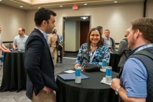
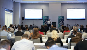
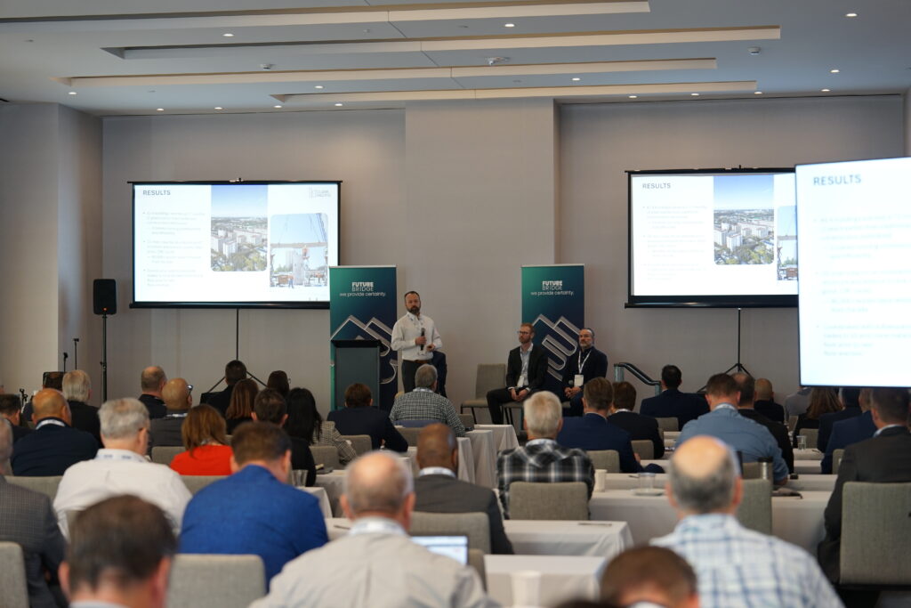
The 2nd Semiconductor Fab Design & Construction Summit – West Coast Edition was an industry-leading event. It was held on March 27-28, 2025, in Phoenix, Arizona. With the semiconductor industry undergoing unprecedented growth, the summit covered issues pertaining to the construction and management of facilities. It included everything from regulatory compliance and sustainability to the shortage of labor and supply chain disruption. So, it offered a comprehensive platform for informed opinions. The summit was a broad cross-section of delegates drawn from semiconductor manufacturing companies, construction and design companies, technology suppliers, consultancies, and government departments. This, in turn, promoted a culture of innovation and partnership necessary for the industry’s long-term growth. This article captures the sessions of the summit and the insightful information shared by industry leaders. It also takes the reader through the sponsors that made this important industry conference a reality.
Sessions at the 2nd Semiconductor Fab Design & Construction Summit – West Coast Edition
The summit boasted a stellar lineup of industry experts. They conducted informative sessions on a wide range of topics concerning semiconductor manufacturing facility design & construction. This section highlights the most significant learnings from each session:
How Arizona Is Building An End-To-End Semiconductor Supply Chain
Speaker: Patrick PTAK, Executive Vice President of Executive Initiatives, Arizona Commerce Authority
The speaker showed Arizona’s incredible evolution as a semiconductor leader. It focused on its 70-year history of chip leadership that has made the state America’s leading semiconductor ecosystem. Furthermore, it conveyed that with over $200 billion of ecosystem investments attracted in just four years alone, throughout the entire semiconductor value chain, Arizona demonstrated incredible growth. The presentation also detailed strategic measures taken to maximize investment opportunities and create a welcoming environment for leading tech companies.
Lessons Learned In 35+ Years Of Cleanroom Construction For Semiconductor Manufacturing
Speaker: Blake HODESS, Chief Executive Officer, Hodess Cleanrooms
Based on three and a half decades of semiconductor experience, the speaker offered a comprehensive retrospective on the development of cleanroom construction from 1988 to the present. Moreover, the presentation highlighted key changes in layouts, processes, and equipment that have reshaped the semiconductor manufacturing landscape. Through illustration of key lessons learned from thousands of projects, the speaker shared insightful recommendations on how to avoid pitfalls and use best practices.
FIRSIDE CHAT: Managing Risk In Facility Design To Protect Project Success And Financial Outcomes
Speaker: Koray KAYA, Director, Facilities Engineering Global Manufacturing & Corporate Facilities, Analog Devices
The speaker presented a thorough overview of risk management methods critical to semiconductor facility design. By considering how facility requirements evolve throughout the project lifecycle, the presentation presented models for prediction and reaction to changing requirements. Additionally, the session covered the cost and schedule impact of design changes. It also demonstrated how good change management could prevent cost escalation.
Water Stewardship In Advanced Manufacturing Plants
Speaker: Kelly OSBORNE, Senior Staff Engineer and Site Water Champion, Intel Corporation
The speaker outlined an end-to-end approach to water resource management in semiconductor fab operation, from the essential early alignment on water stewardship objectives across all stakeholder groups. Strategies for early planning of onsite water reuse and reclamation networks during facility design phases were outlined. This underlines the value of cooperative supplier relationships for optimization of water savings.
Applying Product Manufacturing Practices For Mega Projects
Speakers: Geene ALHADY, President; Loehl O’BRIEN, Project Executive, Clark Pacific
The session looked at how using product manufacturing practices on large-scale semiconductor projects maximizes efficiency and minimizes risks. In addition, speakers elaborated on how integrating construction into production processes facilitates scalable, repeatable elements. They pointed out how modular and prefabrication methods speed up schedules. This is through offsite fabrication and on-site construction parallelization. They also pointed out how DFMLA, standardization, and supply chain techniques assist in controlling costs, eliminating disruptions, and managing labor shortages
Panel Discussion: From R&D To Manufacturing: Planning Your Cleanroom Facility
Speakers: Blake HODESS, Chief Executive Officer, Hodess Cleanrooms; Ben HALLECK, Advanced Manufacturing | Associate Principal, SMRT Architects and Engineers; Thomas GERBO, Principal, Sears Gerbo Architecture
The panel discussion at the 2nd Semiconductor Fab Design & Construction Summit – West Coast Edition discussed challenges of scaling from R&D or startup settings into full-production manufacturing in cleanroom facilities. The speakers talked about strategic process planning, tool matrix development, and major lessons from hundreds of projects. In addition, insights revolved around minimizing risks, maximizing cleanroom design optimization, and smooth scale-up from research to high-volume manufacturing.
Integrating Industry And Academia: Preparing The Next Generation Of Designers And Builders
Speakers: Allan D CHASEY, Associate Professor Emeritus, Del E Webb School of Construction, Arizona State University; Lisa HOGLE, Chief Operating Officer, CREATE (Construction Research and Education for Advanced Technology Environments), and Director, OSHA Education Center, Arizona State University
The session discussed workforce issues in the construction of advanced technology. Furthermore, the session went into how to close the gap between workforce and experience. Speakers also talked about how to link academic programs to industry needs. The session further presented initiatives at Arizona State University. These prepare future designers and builders with the knowledge and experience needed for the future construction environment.
Commercial Roofing And Semiconductor Manufacturing
Speakers: Joe TUBIOLI, Strategic Accounts Manager; John McCALL, Sr. Strategic Account Manager, Carlisle SynTec Systems
The presenters gave a technical presentation of the top-of-the-line intersection between semiconductor commercial roofing solutions and fabbing facilities. The session looked into how high-performance roofing systems contribute to the total integrity and effectiveness of semiconductor fabs. It references the unusual requirements that such facilities present compared to typical commercial buildings.
Bridging The Gap: Enhancing Safety And Efficiency In Semiconductor Facilities With Roxtec
Speakers: Brent BECKER, Business Strategy Manager; Alexander FREEMAN, Infrastructure Segment Manager, Advanced Facilities, Roxtec USA
The session at the 2nd Semiconductor Fab Design & Construction Summit – West Coast Edition centered on enhancing safety and efficiency within semiconductor plants through the utilization of Roxtec solutions. Presenters addressed sealing strategies for cable and pipe penetrations. This is to improve fire protection, reduce contamination threats, and provide operational reliability. Additionally, insights emphasized how Roxtec’s creative designs result in cleaner, safer cleanroom environments within semiconductor fabrication.
Panel Discussion: Modular Construction For Accelerated Facility Development
Speakers: Geene ALHADY, President, Clark Pacific; Pablo RUIZ, Regional Manager, Advanced, Technology Facilities, Austin Commercial; Jesse CRAIG, Project Manager, PACE Systems; Faith ORTIZ, Sr Facilities Mechanical, Engineer, Arizona State University
This panel session discussed next-generation modular construction techniques that dramatically reduce semiconductor facility development project durations. The speakers discussed how pre-engineered modular building elements can reduce construction timelines. This is without sacrificing quality and precision requirements. Moreover, the discussion focused on certain case studies where modular techniques considerably shortened time-to-market for new semiconductor plants.
Evaluating Project Management Approaches From Perspective Of Semiconductor Project Experience
Speaker: Pablo RUIZ, Regional Manager, Advanced Technology Facilities, Austin Commercial
The session analyzed project management strategies within semiconductor projects and contrasted delivery models such as Design-Build and Integrated Project Delivery. Furthermore, the Speaker addressed issues in previous projects and discussed ways of improvement. Main takeaways included tools and methods that improve efficiency, collaboration, and overall performance in the rapidly evolving semiconductor business.
The Case For Design Build Cleanroom Project Delivery
Speaker: Blake HODESS, Chief Executive Officer, Hodess Cleanrooms
The speaker put forward a very strong argument to use Design-Build delivery methods on cleanroom projects. The session further went into how these delivery methods were greatly beneficial in the construction of semiconductor facilities. Furthermore, the presentation drew attention to the way the single-point-of-responsibility model simplifies the management of a project. This is with lesser contractual complexity and possible disputes.
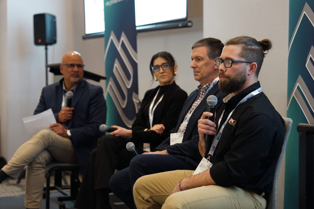
Innovations In Semiconductor Manufacturing Technologies And Facility Design
Speaker: Prashant PATIL, Ph.D. – CEO & Founder, Micromize, Inc
The session identified new developments in semiconductor production and building design. Furthermore, the speaker highlighted top-of-the-line production equipment, the most significant design factors of high-tech plants, and security measures to improve safety and conformance. Innovative trends in laser technology were also presented. It showcased its application as a means to drive efficiency and accuracy in processes used in making semiconductors.
Digital Twin In Advanced Package Manufacturing: The Role Of DOE Simulation And Multi-Physics Integration
Speaker: Woopoung KIM, Corporate EVP, Head of Packaging Solution Center, Samsung Electronics
The speaker gave an advanced analysis of digital twin technology and its revolutionary power in leading-edge semiconductor packaging manufacturing. Moreover, the talk explained how design of experiments (DOE) simulation approaches merge with multi-physics modeling. This is to form detailed digital models of physical manufacturing systems.
Managing Contractor Risk In Semiconductor Construction & Operations
Speaker: David TIBBETTS, Chief Safety Officer, Highwire
The session at the 2nd Semiconductor Fab Design & Construction Summit – West Coast Edition discussed the pivotal role of contractor management in semiconductor construction and operations. Furthermore, the speaker elaborated on typical gaps in conventional methods and how they affect project success. Moreover, the speaker outlined strategies employed by leading manufacturers to reduce risks. In addition, key takeaways included best practices that improve efficiency and result in substantial insurance savings in semiconductor projects.
Applying Quantum Physics Principles In Safety: Designing A Self-Sustaining System
Speaker: Eldad A. SHAHAR, Semiconductors EHS Subject Matter Expert | VP, HBC-Semicons
The session considered the application of principles of quantum physics to designing an autonomous safety system. Furthermore, the presenter addressed the business rationale for such a system and how it addresses escalating costs, labor volatility, and disruptions. Moreover, emphasizing the move from control to stewardship, the session illustrated how concepts from quantum mechanics can help develop a robust, accountable safety culture in organizations. It includes tunneling and entanglement.
Delivering Projects On Budget And Schedule Using Collaborative Agreements
Speakers: Neil KAUFMAN, Director of Project Integration; Haley ROGERS, Lean Coach for Semiconductor, Design & Construction Project, Boulder Associates
The speakers shared best practices for project delivery based on collaborative agreement frameworks. These reliably yield on-budget, on-schedule results. Furthermore, the presentation looked at how conventional contractual models tend to foster adversarial relationships that threaten project success. The session also compared this to collaborative models with aligned incentives among all parties.
Contamination Control And Management In Manufacturing
Open Discussion Session
This open discussion session allowed for an interactive examination of contamination control issues and resolution in semiconductor manufacturing environments. Moreover, learners shared knowledge of changing cleaning standards and how these are implemented within different facilities.
Operational Strategies For Semiconductor Manufacturing Facilities
Speaker: Mousumi BHAT, VP Sustainability Programs, SEMI
The seminar addressed operational techniques for semiconductor manufacturing plants, design, and construction issues. The speaker addressed the installation of automation and robotics to enhance production efficiency. The session further went into supply chain aspects and how to achieve sustainability in facility design. Furthermore, strategies to develop cost-cutting financial models without compromising on quality were also discussed. It considered project feasibility and long-term success.
Who Were The Sponsors For The 2nd Semiconductor Fab Design & Construction Summit – West Coast Edition?
The 2nd Semiconductor Fab Design & Construction Summit – West Coast Edition’s success was highly boosted by industry-leading sponsors. They provided their know-how and solutions to the summit. Moreover, these organizations are the semiconductor facility design, construction, and support services industry leaders. So, let us take a glance at them:
Hodess Cleanrooms – Platinum Sponsor
North America’s most prominent single-source provider of Cleanroom lifecycle expertise, Hodess Cleanrooms brings critical environment management expertise from development and management to evolution. Furthermore, they deliver turnkey services ranging from design and engineering to construction, protocol strategy, certification, testing, and facility retrofit in semiconductors, batteries, medical devices, defense, biologics, and pharmaceuticals. Through the summit, they shared insightful lessons from their wealth of industry experience. They discussed pragmatic methods for cleanroom construction and design-build project delivery approaches that meet operating parameters, budgets, and timelines.
Clark Pacific – Gold Sponsor
Clark Pacific is a pioneer in producing prefabricated building systems in an efficient, high-quality fabrication method. Their product focus delivers integrated systems with flexible design, budget protection, accelerated project schedules, and minimized project vulnerability. Moreover, committed to sustainability, they produce energy-efficient, durable solutions to meet individual client specifications. During the summit, they exchanged knowledge regarding modular building methods and production methods for improving facility construction. This showcased how their techniques shorten construction timelines and eliminate project hazards.
Carlisle SynTec Systems – Silver Sponsor
Carlisle SynTec Systems is a world-class single-ply roofing systems company with over four decades of history and nine billion square feet of sold roofing membranes. Furthermore, their R&D has led the way in innovations for EPDM and TPO membranes. It consistently ranks at the top of industry surveys for product quality, innovation, and roofing technology. Moreover, at the 2nd Semiconductor Fab Design & Construction Summit – West Coast Edition, they presented expert information regarding commercial roofing applications unique to semiconductor manufacturing facilities. It leveraged their industry knowledge to meet the distinct needs of fab construction.
Highwire – Bronze Sponsor
Highwire‘s prequalification and field applications give manufacturers and contractors end-to-end subcontractor risk assessment capabilities above and beyond routine compliance, assessing safety, financial stability, and operating capacity. Unlike typical contractor management systems, their integrated suite enables full-lifecycle risk reduction. This is with actionable mitigation plans monitored through inspection tools. At the summit, they illustrated how their solutions avoid delays, reduce costs, and improve safety. They shared best practices for contractor risk management specific to semiconductor construction and operations.
HBC Semicons – Bronze Sponsor
HBC Semicons provides Environmental Health and Safety services to the semiconductor sector with 17 years of specialized experience. Furthermore, the organization facilitates compliance and occupational safety through in-depth semiconductor fabrication process knowledge and associated hazards. Moreover, integrity-focused, sustainable, and innovative in approach, they navigate customers through EHS intricacies. Their 2nd Semiconductor Fab Design & Construction Summit – West Coast Edition presentation emphasized safety system design principles. It highlights their experience in developing self-existent safety cultures. It also illustrates their established record as a reliable partner in ensuring safe and sustainable semiconductor production.
Roxtec – Bronze Sponsor
Roxtec Sealing Solutions offers fire, gas, and water protection in shipbuilding, oil and gas, energy, infrastructure, and manufacturing sectors. Furthermore, their entry seals adapt to fit different structures. This ensures safety in hazardous places. Moreover, their Multidiameter™ technology allows flexible sealing for various cable and pipe diameters with expansion potential. The Roxtec Transit Designer™ also optimizes product choice and improves engineering processes. They presented at the summit how to improve safety and efficiency in semiconductor fabs. This showcases how their sealing solutions meet critical protection requirements in fab environments.
Boulder Associates – Presenting Partner
With more than 40 years of healthcare, senior living, and life science design experience, Boulder Associates has extensive knowledge in industrial, manufacturing, and institutional construction management consulting. Furthermore, their BA/Science team offers process-driven design thinking, collaboration, research, and innovative business solutions. They are experts in managing collaborative agreements for complicated engineering and construction projects. They exchanged insightful viewpoints on project delivery strategies that place complex semiconductor projects within budget and schedule using efficient collaborative agreements during the 2nd Semiconductor Fab Design & Construction Summit – West Coast Edition.
Cupix – Exhibiting Partner
Cupix is a leading 3D digital twin platform for owners and builders. It facilitates end-to-end management of jobsites through mobile apps and 360-degree camera technology. Moreover, their cloud-based solution facilitates remote site exploration, progress tracking, BIM analysis, 3D measurement, and geospatial annotation. At the summit, they showcased how their technology provides collaboration, confidence, and control. This is to enable project teams to achieve timelines, budgets, and targets across the project life cycle. It also reflects their dedication to building digital twin infrastructure and making construction processes smarter.
ATS – Exhibiting Partner
ATS Products Inc. has been a global industry leader in fire-resistant and corrosion-resistant FM4922-approved exhaust systems since 1981. It sets industry standards as the first to survive the FM4922 duct fire test. Furthermore, they offer PFAS-free FXP™ FRP ducts with worldwide recognition for corrosion and fire resistance, available in sizes from 2″ to 156″ diameter on four continents. At the summit, they displayed their specialized exhaust systems for semiconductor facilities. This is with emphasis on how their 50+ years of experience drives their innovative, dependable, and sustainable solutions for semiconductor manufacturers.
Garney – Exhibiting Partner
Garney Construction has been at the forefront of water and wastewater infrastructure since 1961. They showcase expertise in design-build and CMAR services. They partner with municipal, federal, industrial, and private clients to build efficient, environmentally friendly infrastructure systems. Additionally, their engineering, project planning, and construction skills place them well to take on cost-effective, environmentally friendly water system development. During the 2nd Semiconductor Fab Design & Construction Summit – West Coast Edition, they proved their experience in water infrastructure necessary for semiconductor production. This highlights their creative methods and collaboration-based approach that makes them a reliable name in critical utility system building.
To Sum Up
The 2nd Semiconductor Fab Design & Construction Summit – West Coast Edition provided in-depth information on major industry issues and innovative solutions. Spanning sustainability, modular building, risk management, and collaboration, it had insightful takeaways for semiconductor facility development professionals. Bringing together specialists from all corners of the ecosystem, the summit created knowledge sharing and enduring relationships.
As the sector innovates, participating in subsequent sustainability-driven semiconductor gatherings remains essential. This is to keep pace with developing trends, technologies, and best practices that will define tomorrow’s manufacturing plants. So, make sure you check out the upcoming summits and register!

