")
The Semiconductor Fab Design, Engineering & Construction Summit USA 2026 is a leading semiconductor fab construction summit bringing together industry leaders in fab design, engineering, and manufacturing infrastructure in Washington, DC.
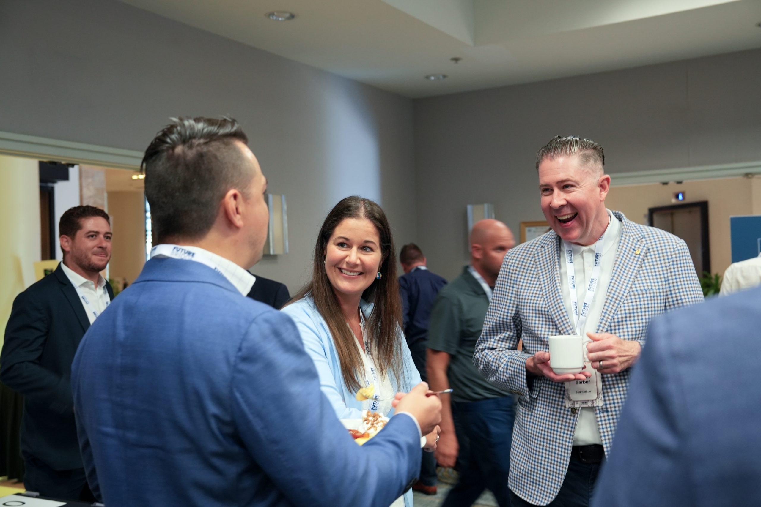
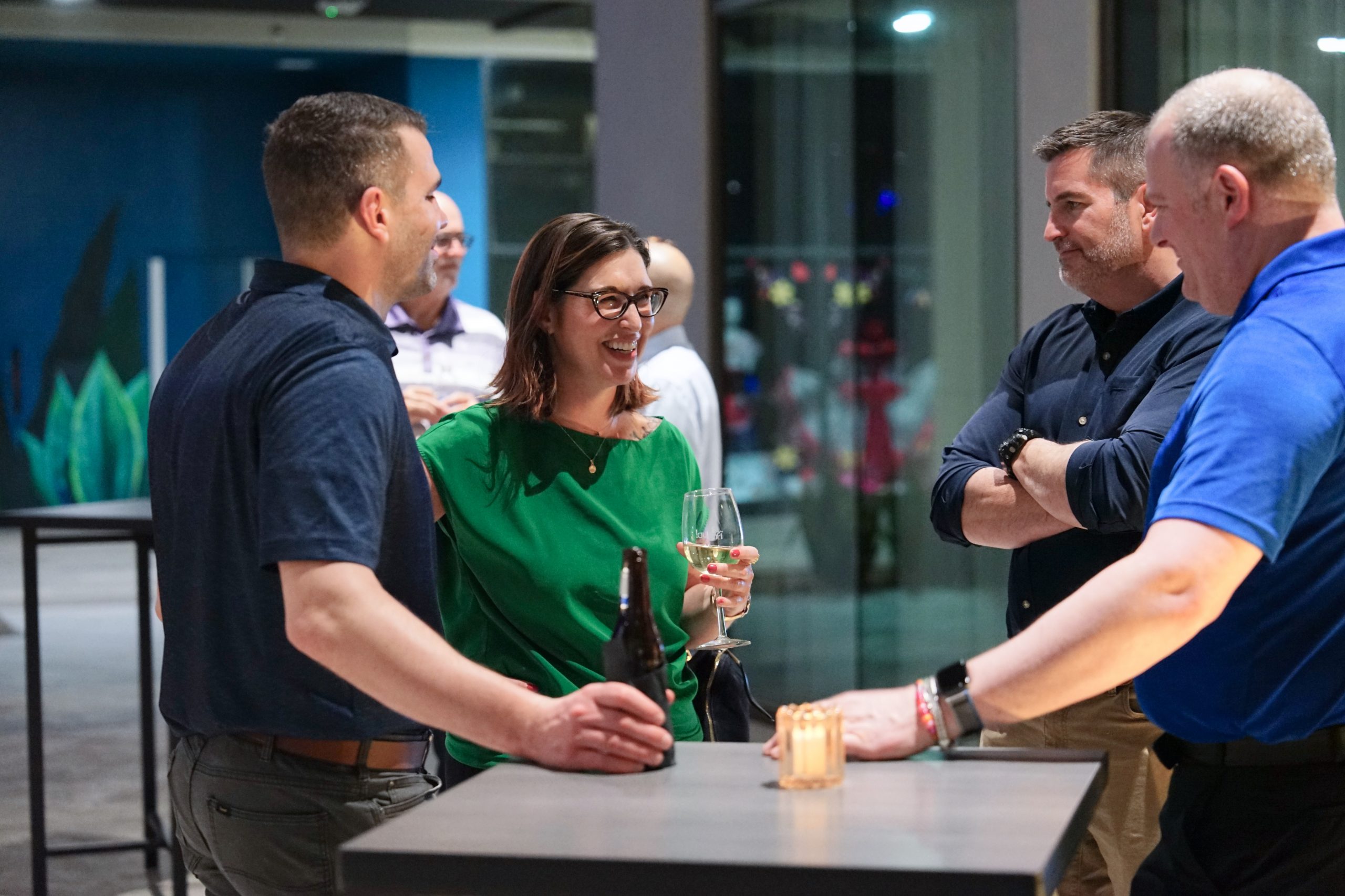
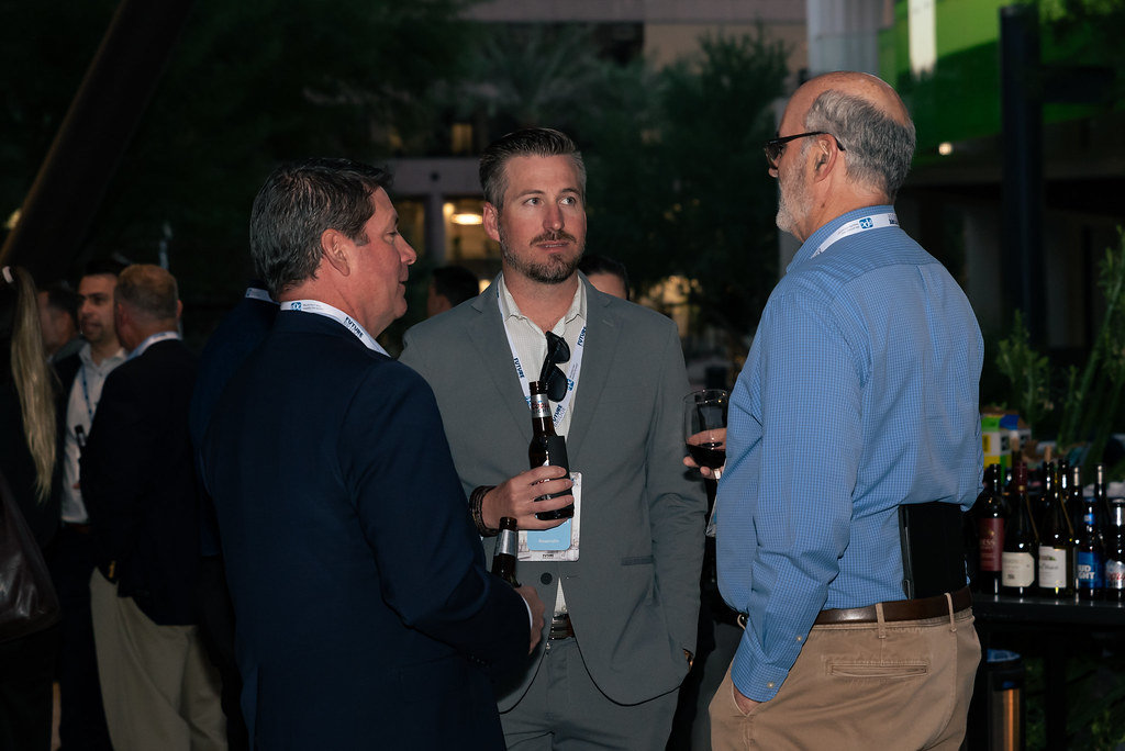
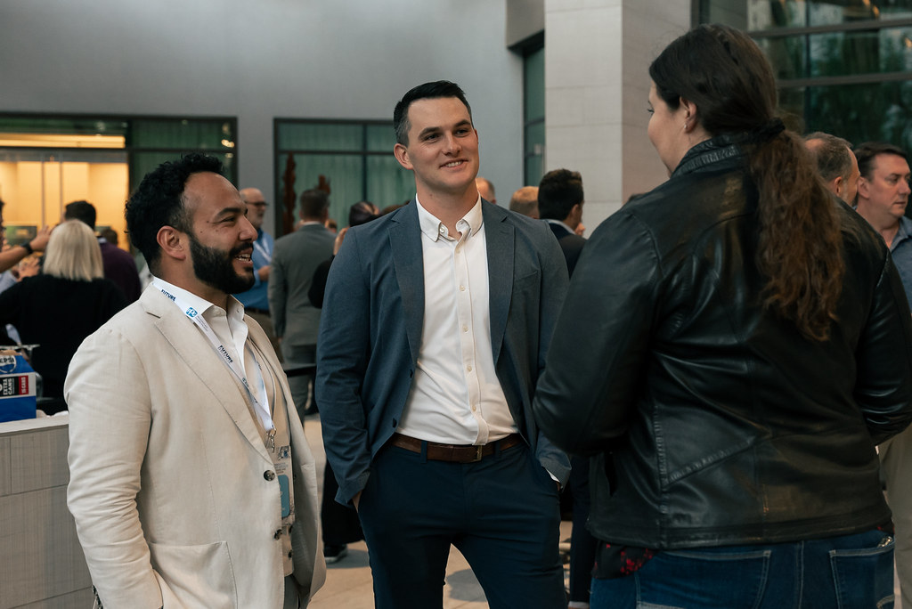
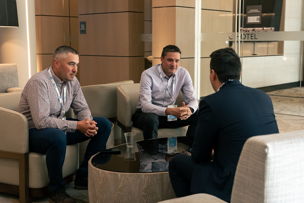
Business Networking
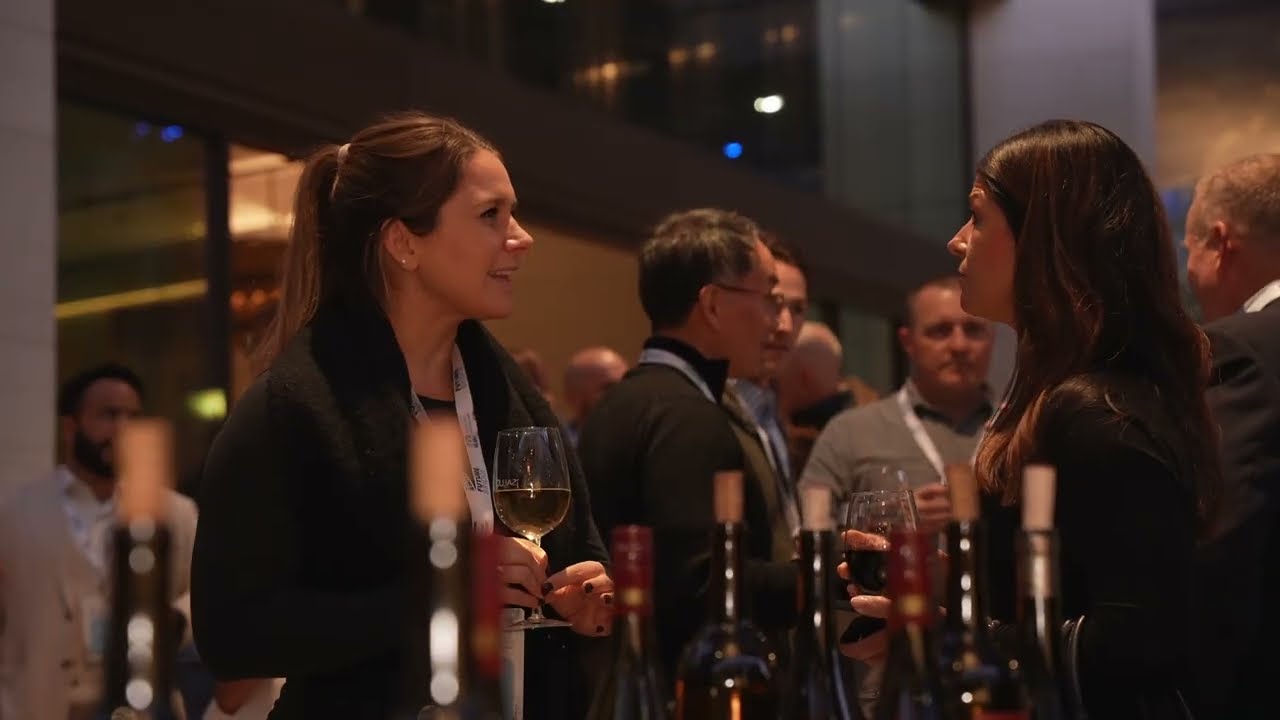
Future Bridge is proud to offer ample networking opportunities during our event. The agenda includes pre-arranged 1-to-1 face meetings during a Coffee and Ice-breaking session designed to foster meaningful connections and facilitate interactions among attendees.
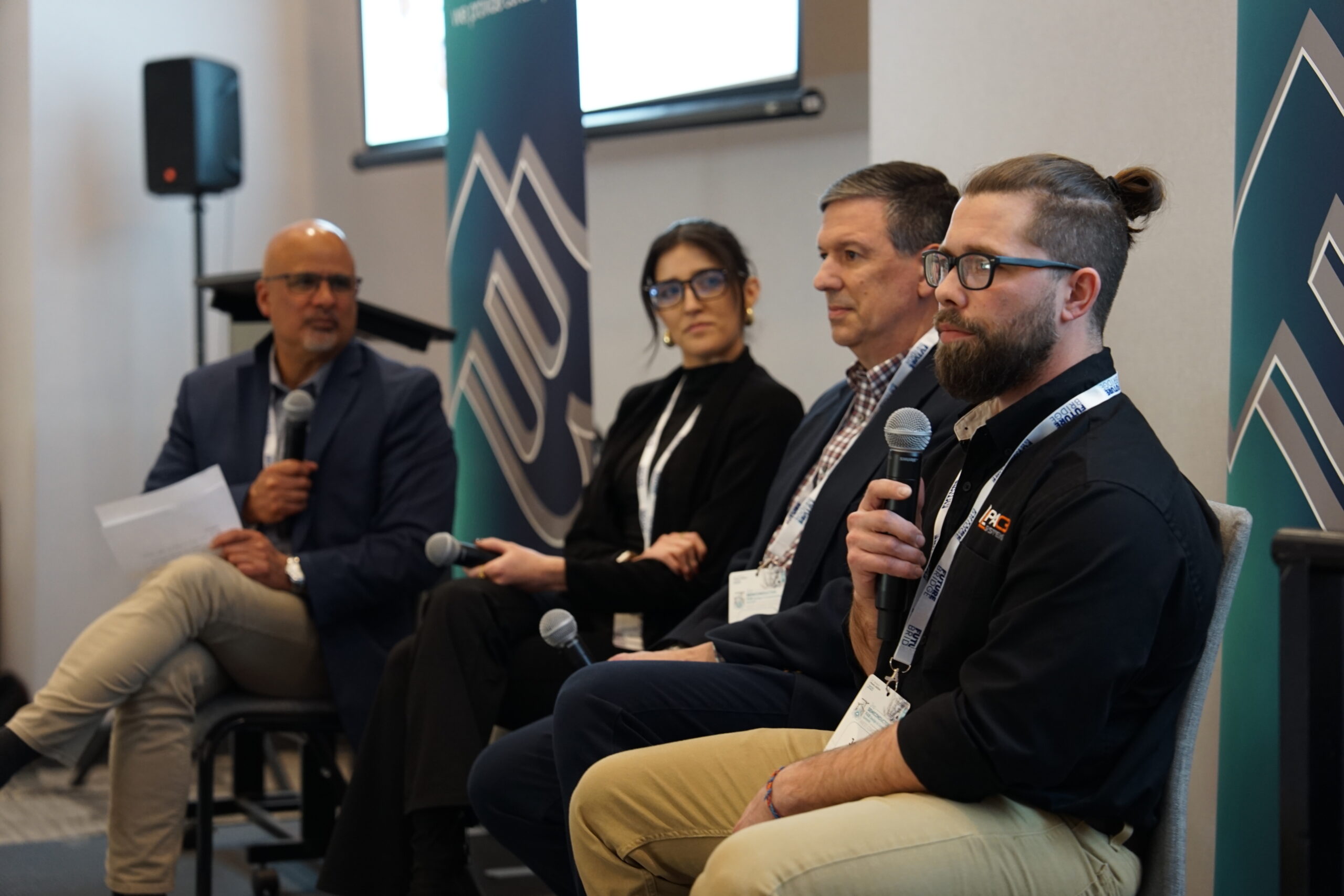
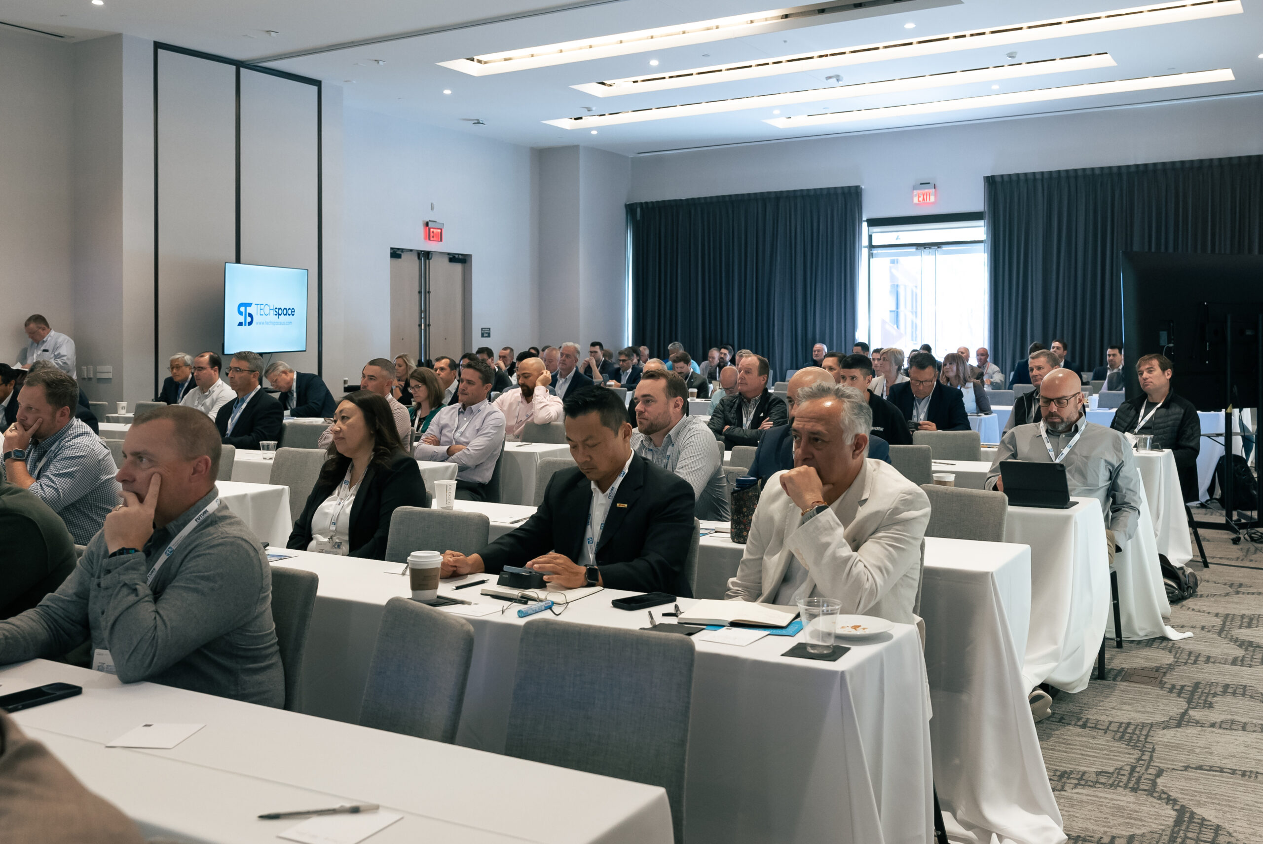
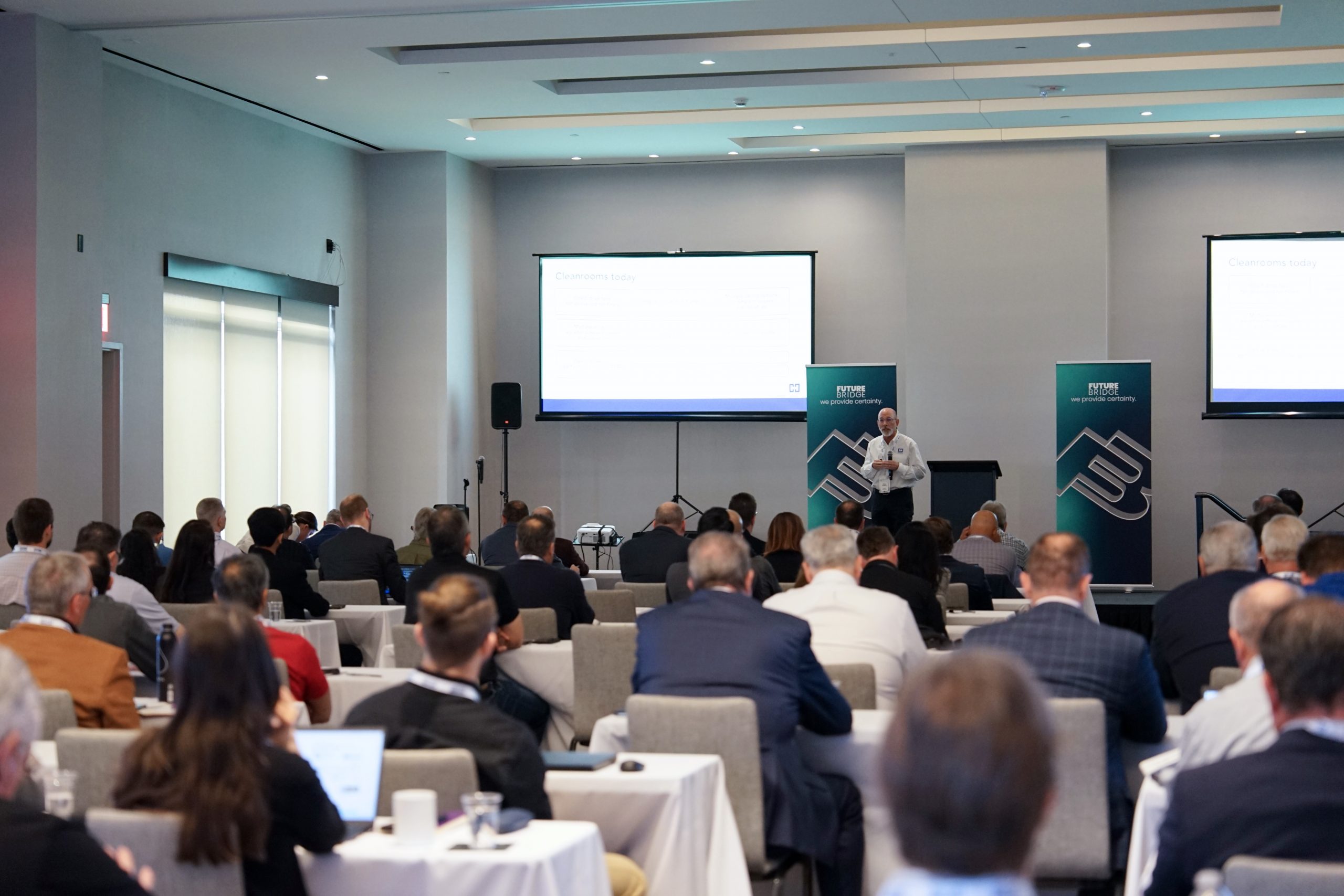
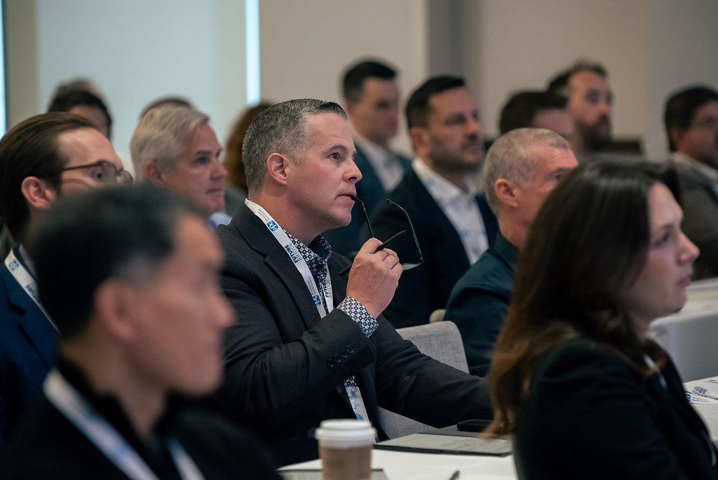
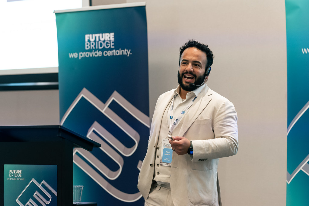
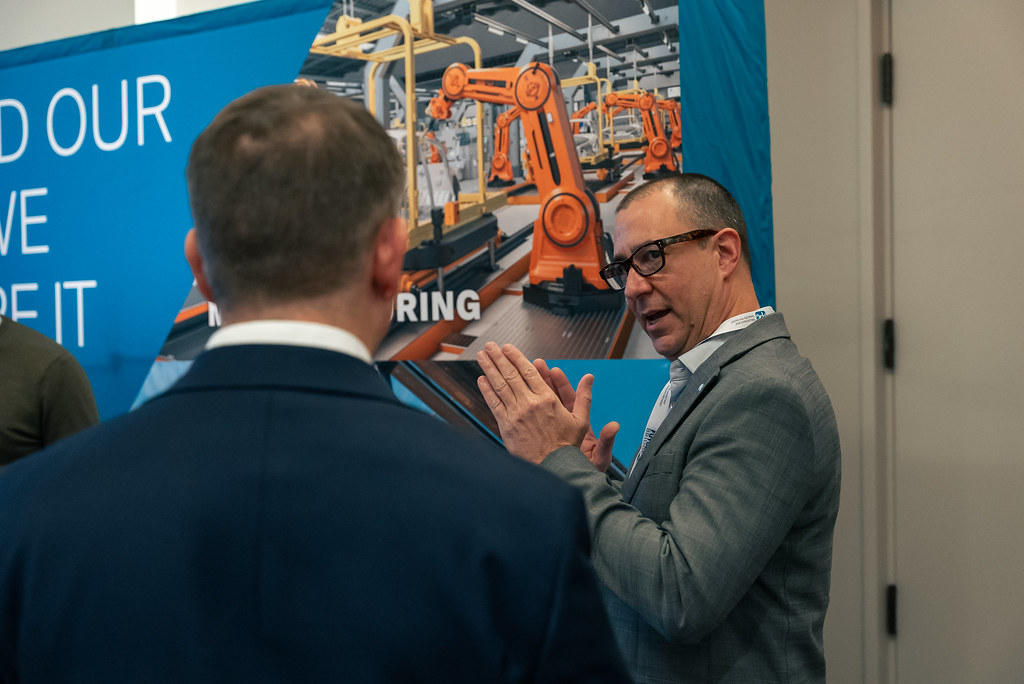
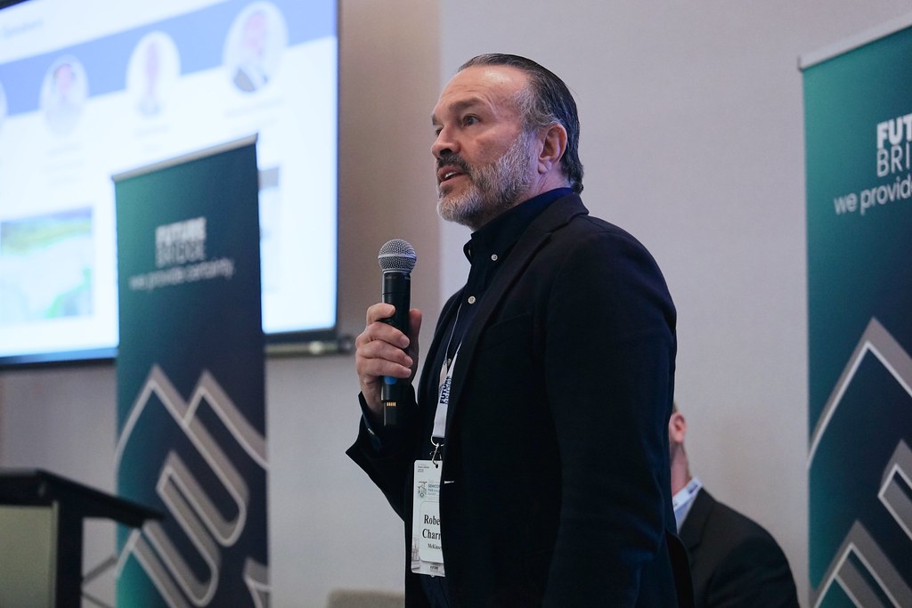
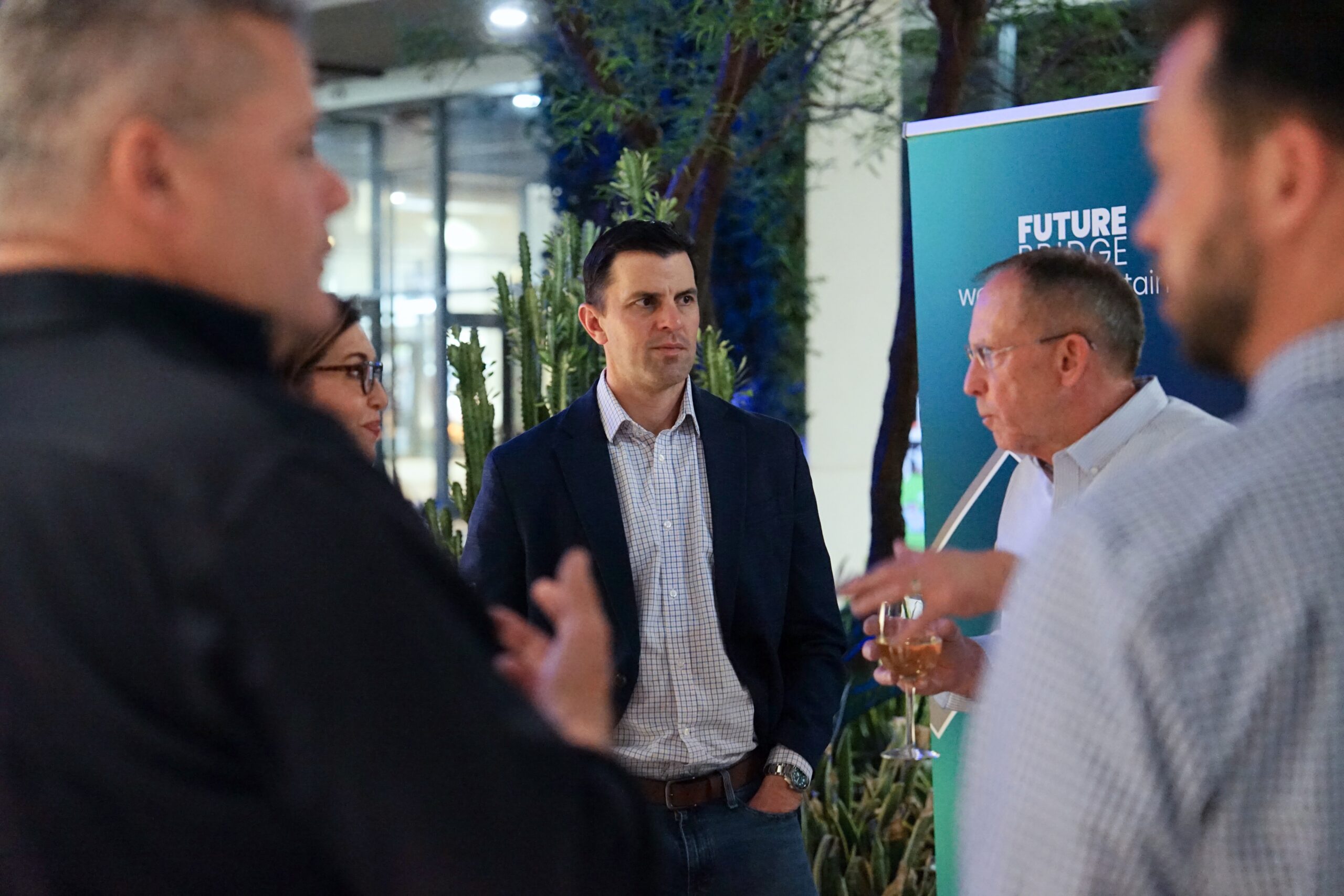
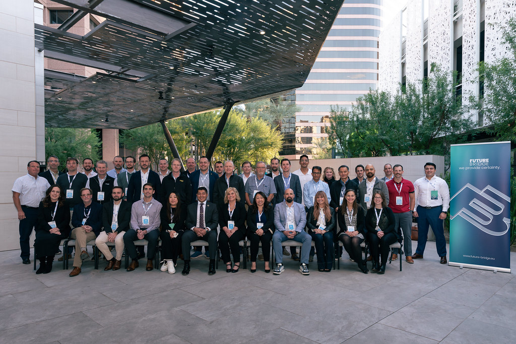
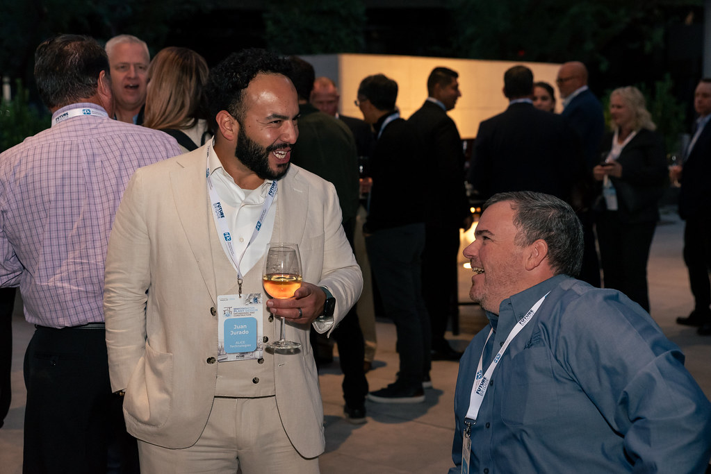
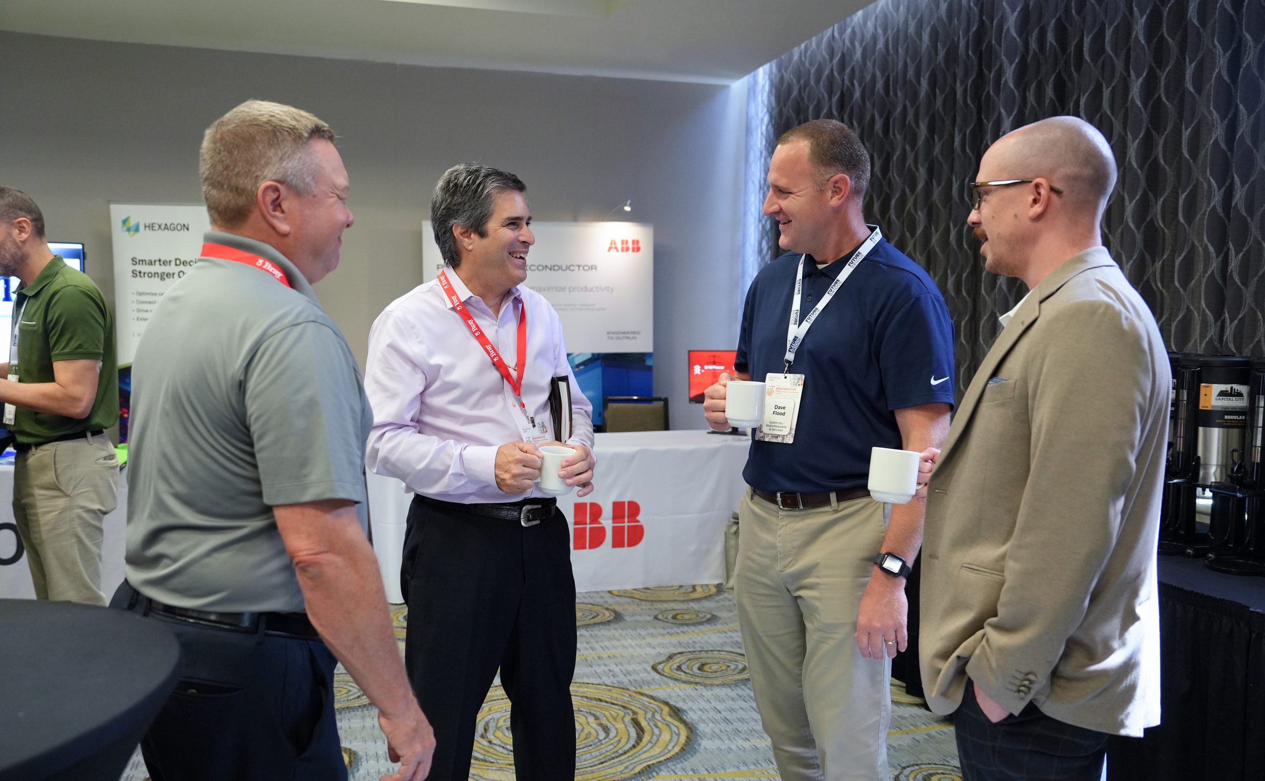
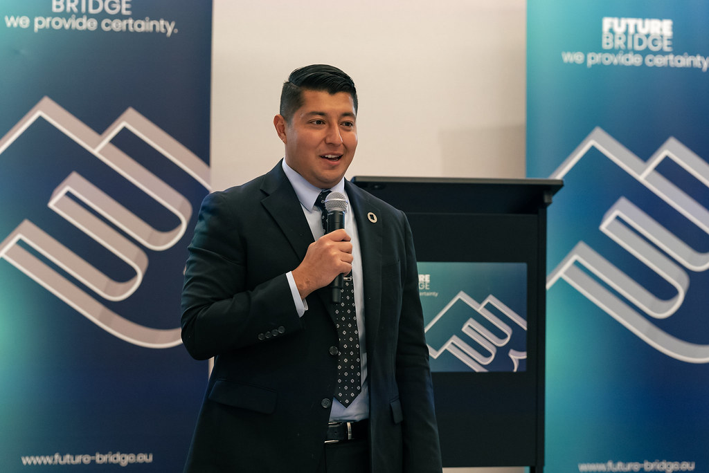
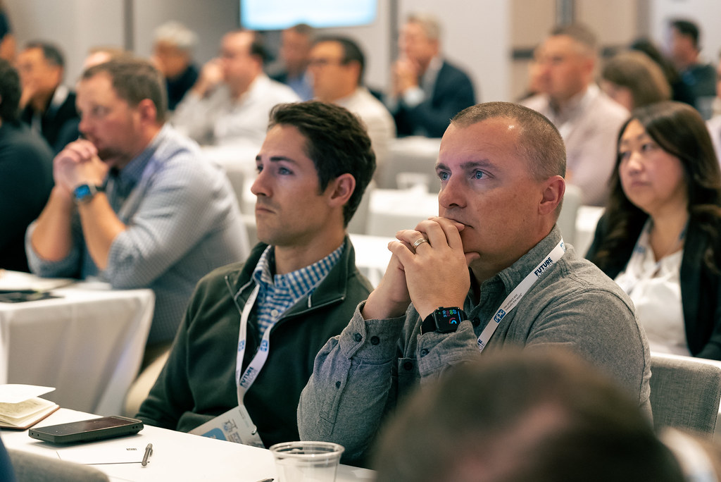
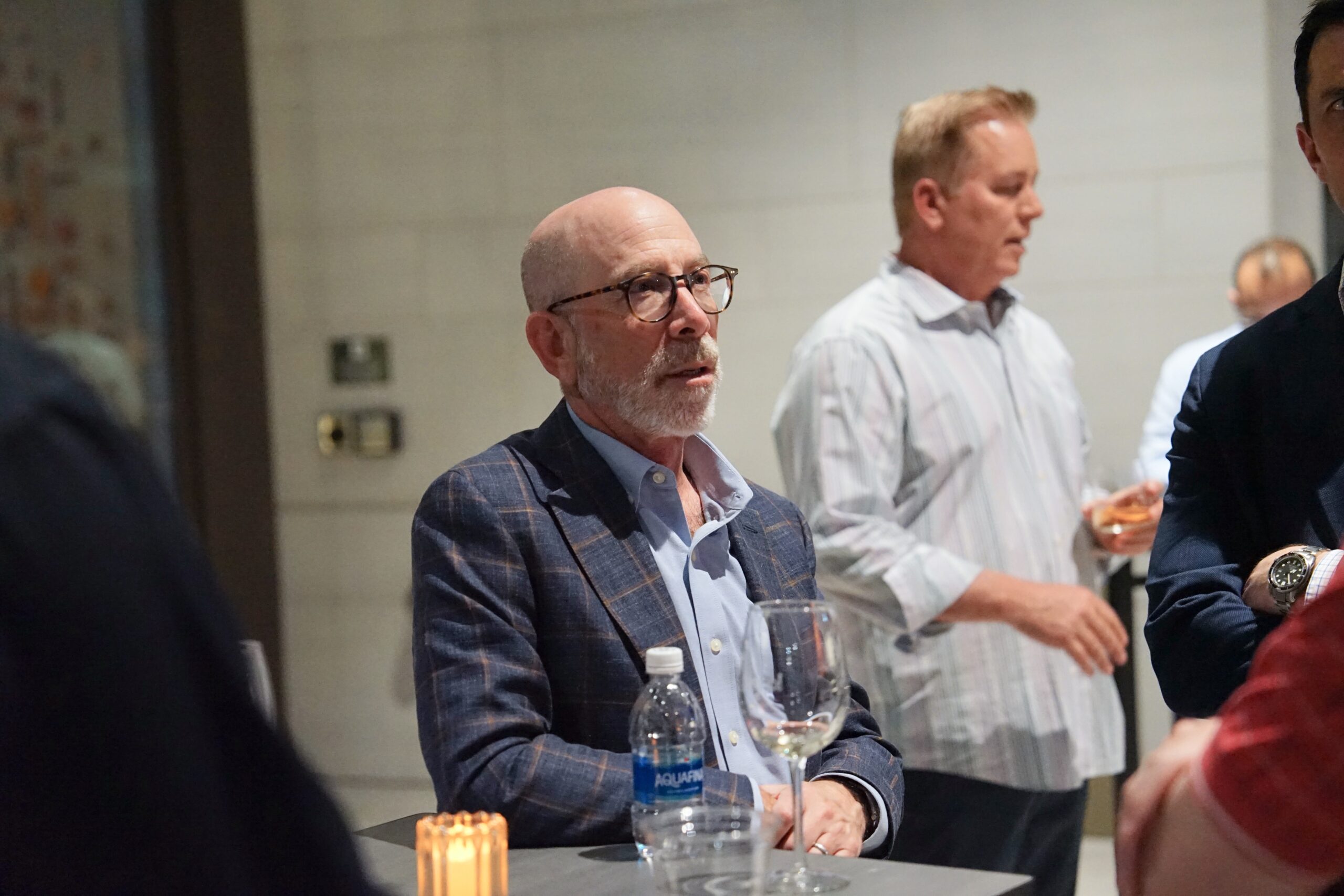
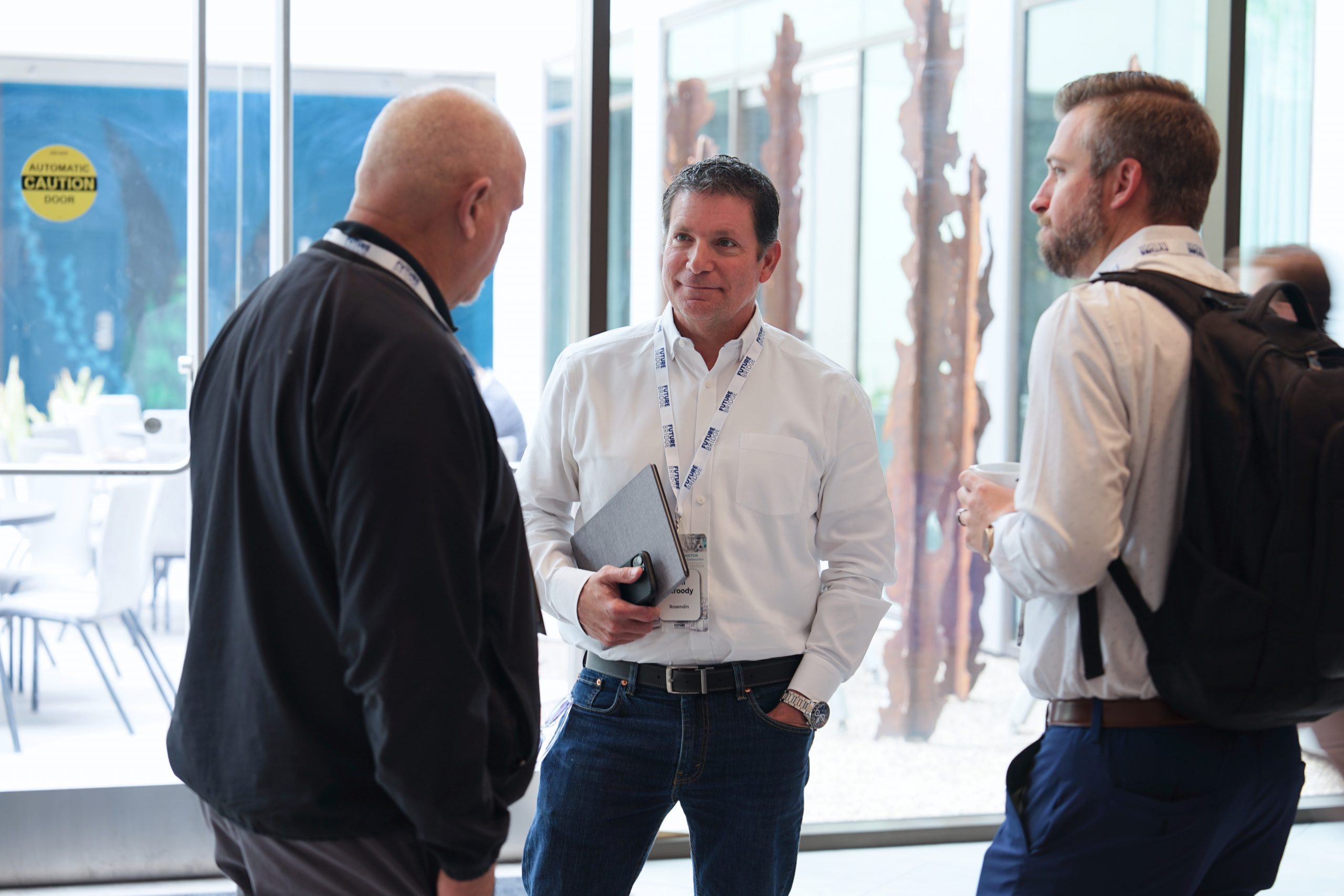
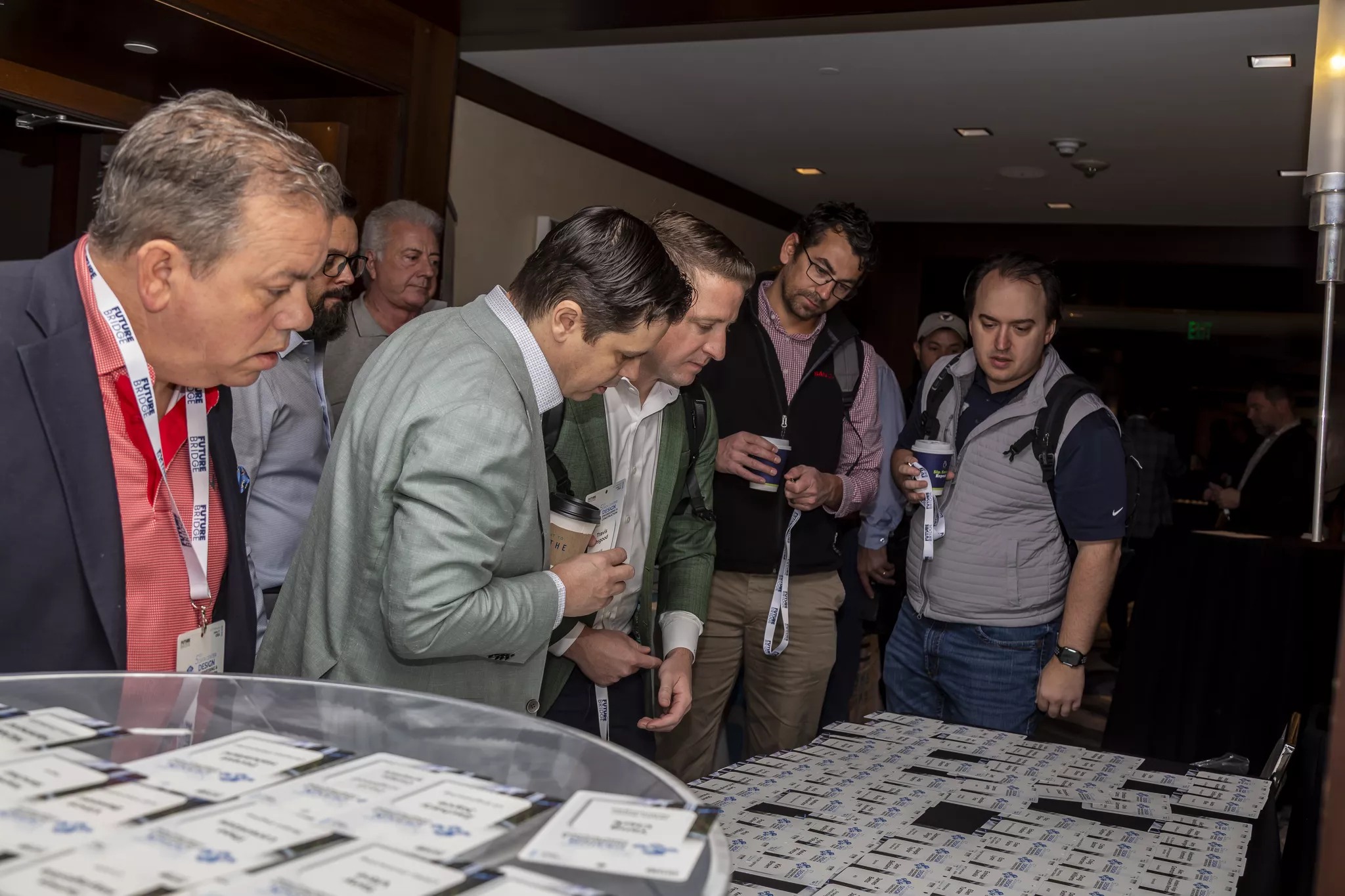
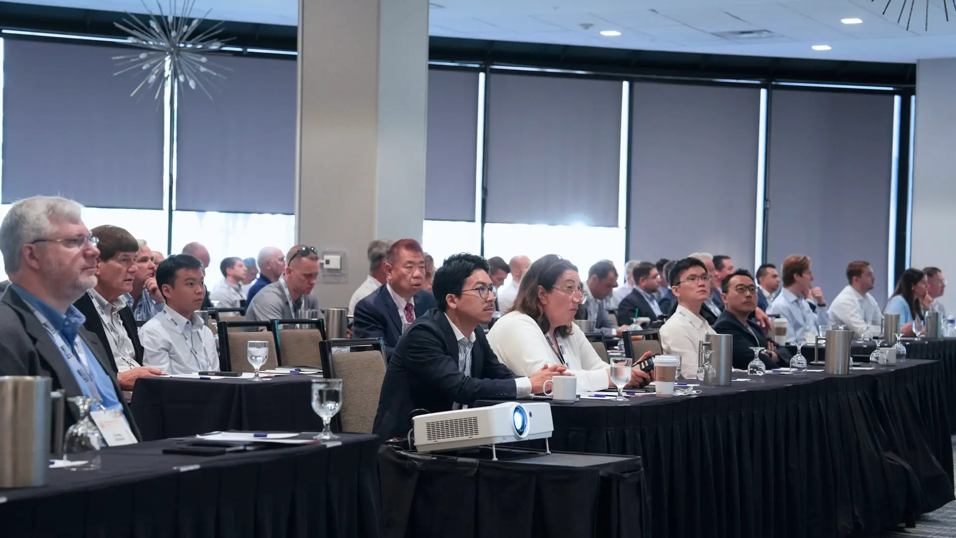
From Previous Summits
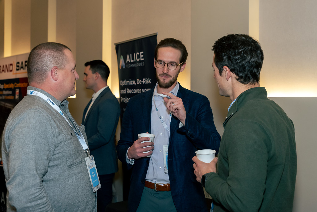
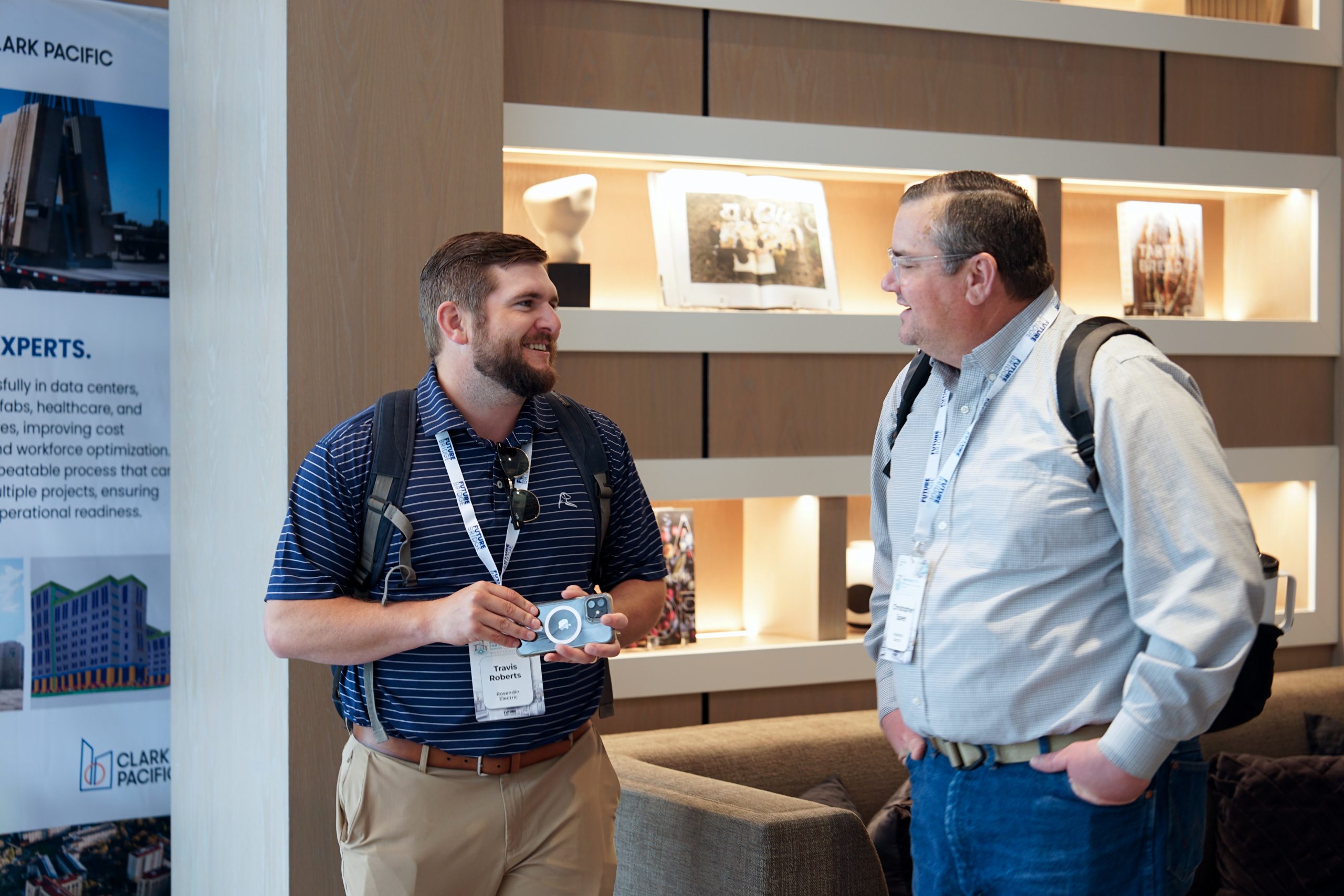
Participants will have the opportunity to engage in focused discussions, exchange ideas, and establish new relationships during both structured sessions and informal breaks throughout the two-day program.
Secure Your PlaceBusiness Networking at the Semiconductor Fab Design, Engineering & Construction Summit
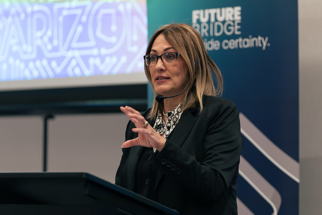
From Previous Summits


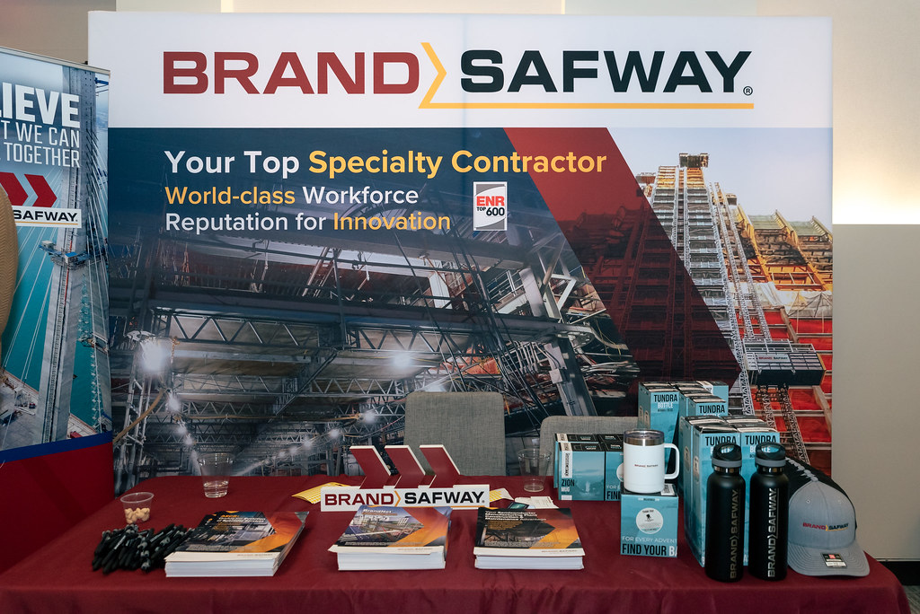
Speakers' Companies

Event Sponsors
Event Venue & Accommodation
Fairview Park
King Bed
Single Occupancy
Reservation deadline: June 8, 2026 (based on availability)
Falls Church Marriott Fairview Park is ideally located in the Washington metropolitan area, offering convenient access to both downtown Washington, D.C., and Northern Virginia's key business districts. The hotel is situated approximately 25 minutes by Metro and 20 minutes by car from Ronald Reagan Washington National Airport.
Situated near major highways and just a short distance from the Mosaic District, the hotel provides guests with easy access to shopping, dining, and entertainment options. Visitors can also explore nearby attractions such as the National Mall, Arlington National Cemetery, and Tysons Corner.
The hotel is well connected to public transportation, making travel throughout the region simple and efficient. With its comfortable accommodations, modern amenities, and prime location, it is an excellent choice for both business travelers and guests looking to experience the vibrant culture and attractions of the Washington metropolitan area.
Reserve at Special RateTo make a reservation at a special rate, please contact support@future-bridge.eu


Highlights from our previous summits — connecting the semiconductor fab design and construction community across multiple editions.

Relevant Events
Brings together senior leaders in semiconductor fab design, engineering and construction across Asia-Pacific. Focuses on fab expansion strategies, power and utilities infrastructure, UPW and wastewater systems, cleanroom engineering, and modular construction.
Focused on facility architecture, power scaling and operational models for AI-ready deployments. Deep technical and strategic insights across the full lifecycle of building and retrofitting AI-ready infrastructure. Attendees engage with industry leaders, operators, GPU ecosystem providers, and engineering experts.
Brings together data center owners, developers, engineers, and operators in Ashburn to explore AI-ready, high-density, and sustainable infrastructure. A focused agenda on advanced cooling, power availability, modular design, and future-ready construction strategies.