")
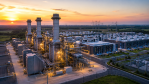


The 5th Semiconductor FAB Design, Build & Facility Operations Summit recently wrapped up in Phoenix. It was a massive success for anyone involved in high-tech construction. Today, the industry is moving faster than ever. Therefore, staying on top of semiconductor design is the only way to remain competitive. Throughout the event, speakers shared how they are using AI and new building methods to hit record speeds.
Market Outlook and Strategic Planning
The summit started with a look at the road ahead. Matt Gulley, Vice President and GM from Turner Construction Company, talked about the U.S. fab expansion through 2027. Furthermore, he explained how the Chips Act and AI data centers are changing the game. Because of these shifts, semiconductor fab design now requires a much stronger supplier ecosystem.
To keep projects moving, Mike Lindell (Program Superintendent) and Adam Tarr (OSM Director) from Hoffman Construction discussed Builder-Driven OSM. They argued that a builder’s influence is a must for a positive program strategy. By moving work away from the site, teams ensure a safer and more efficient hand-off to operations. So, this approach truly changes how we think about the initial stages of semiconductor design.
Power, Reliability, and Data
Power is a huge topic when you are building a factory. Paul Olis, Product Market Manager from ABB, introduced voltage sag protection as a strategic asset defense. Moreover, he explained that power quality is vital for fab reliability. Similarly, Sheida Khorrami, Senior Global Facility Electrical Engineer from Micron Technology, showed how to optimize electrical infrastructure. She focused on future-proofing semiconductor fab design by upgrading transformer capacity for next-generation tools.
Shantam Chavan, Product Marketing, Homologation and Business Development, also from ABB, reinforced these ideas by focusing on the resiliency of electrical equipment. He made it clear that homologation is the backbone of a successful plant. Meanwhile, Pankaj Sharma, Sr. Manager Silicon Design Engineering from AMD, explored how “Design for Test” (DFT) impacts high-volume manufacturing. Additionally, the speaker shared that using AI in DFT helps teams improve yield and accelerate the manufacturing ramp.
AI and Operational Excellence
Data is the new secret weapon for semiconductor fab design. Deepshikha Shekhawat, Business Intelligence Program Manager, from AMD, presented a framework for business continuity in a volatile landscape. She showed how data-driven insights help managers strengthen crisis response. Following her, Paul Schneider from Intel demonstrated how digital twins and AI streamline factory operations. As a result, these virtual models cut down cycle times and improve capacity planning.
Later, experts like Paul SCHNEIDER (Director of Automated Factory Solutions, Principal Engineer, Intel) and Pankaj SHARMA (Sr. Manager Silicon Design Engineering, AMD) joined a panel to discuss the operational realities of advanced node fabs. They talked about using robots and AGVs to reach near “lights-out” operations. Moreover, this level of automation is now a central part of semiconductor facility design.
Darin Hart, Senior Vice President, Advanced Technology from Suffolk Construction, also shared a fireside chat on using technology to build the world’s most technical projects.
Workforce and Life Cycle Strategy
The human side is just as important as the tech. Allan D. Chasey from Arizona State University discussed integrating industry knowledge into the classroom. We need a strong workforce to support the future of semiconductor fab design.
Furthermore, Kelsyn Rooks from Cupix then showed how scaling spatial intelligence tracks site progress in real time.
Finally, Brian Hwang from Eastern Builders Inc reminded the audience that they are “more than builders.” He explained that partnerships and culture determine if a project stays on schedule. The summit ended with a site visit to the ASU Factory. There, attendees saw these concepts in action. As a result, it was a great way to see the reality of semiconductor fab design today.
Who Were the Event Partners For the 5th Semiconductor FAB Design, Build & Facility Operations Summit?
Meet the tech leaders and engineering experts providing the vital tools and systems to de-risk our most ambitious builds.
ABB – Gold Sponsor
ABB provides the technical muscle for modern electrification and industrial automation. They have split their expertise into four key buckets, like power distribution and robotics. Consequently, they help manufacturers automate production lines and scale power needs safely. At the 5th Semiconductor FAB Design, Build & Facility Operations Summit, they showed how to make operations more efficient. Furthermore, their goal is to mesh digital tools with traditional engineering. This creates a more sustainable factory. They focus on resource efficiency to help every semiconductor fab design succeed in the long run.
Vacuum Barrier Corporation (VBC) – Exhibiting Partner
If you move liquid nitrogen, you likely know VBC. They built their business around dosing and vacuum-jacketed piping. Their “NITRODOSE” systems are a great example of clever engineering. They inject a precise drop of nitrogen into containers to create pressure. This stops thin-wall bottles from collapsing. Moreover, on the industrial side, their vacuum-insulated piping sets the standard for moving cryogenic fluids. It ensures almost zero thermal loss. So, this reliability is vital for the sensitive thermal environments often found in semiconductor facility design.
Swagelok – Exhibiting Partner
Swagelok is famous for high-pressure tube fittings and valves. However, they have evolved into a broad service provider. Furthermore, they make components for extreme environments like hydrogen plants and semiconductor fabs. In these settings, a leak is a major failure. For that reason, reliability is critical for semiconductor fab design. Beyond parts, they offer “Custom Solutions” where engineers design entire assemblies. They also perform leak-detection audits on-site. As a result, this confirms that teams have installed every fluid-handling system properly and safely for the long term.
AirJoule Technologies – Exhibiting Partner
AirJoule is doing something truly different with water harvesting. They do not use typical refrigerants. Instead, they use a special Metal-Organic Framework (MOF) to pull distilled water right out of the air. As a result, this makes their system very energy efficient. It is a lean way to run a facility. More importantly, it reduces the need for heavy cooling. This is a smart move for semiconductor fab design because it works even in arid climates. Moreover, it offers a fresh way to get moisture for HVAC systems.
Yokogawa – Exhibiting Partner
Yokogawa provides the “control brains” for industrial plants. They are best known for Distributed Control Systems (DCS) that keep massive facilities running safely. They also offer high-precision hardware like flow meters and analyzers. These devices provide the real-time data needed for process optimization. At the same time, they focus on connecting plant data with enterprise intelligence. This helps plants move toward autonomous operations. Additionally, their work is a perfect fit for the data and cybersecurity needs of modern semiconductor facility design.
VEGA – Exhibiting Partner
VEGA specializes in measuring what is happening inside a tank. They pioneered 80-GHz radar technology for tough environments. Furthermore, this tech works through steam, dust, and high pressure. Because the sensors are non-contact, the product does not foul them up. They designed their hardware to be “plug and play” with current systems. This gives chemical or water plants a simple way to track inventory. It is an essential tool for the precision required in semiconductor fab design.
Foresight Technologies – Exhibiting Partner
Foresight built a predictive platform for high-stakes construction. Their AI digs into schedules to find hidden risks and predict delays. As a result, project leaders see problems before they actually happen. It acts as a single source of truth for executives. This automates reporting and gives a clear look at schedule health. By turning raw data into a forecast, the platform keeps teams aligned. So, this helps them avoid the budget overruns that often plague semiconductor fab design.
ATS Duct – Exhibiting Partner
ATS Duct leads the industry in fire-safe and corrosion-resistant exhaust systems. Their flagship composite duct meets strict cleanroom standards. This matters because you can run an exhaust system without internal sprinklers. Engineers design these systems to handle hazardous fumes found in wastewater or fab facilities. They also developed a special resin system for leak-proof connections. As a result, teams avoid using hazardous resins in sensitive areas. This is a major win for the safety of semiconductor design.
To Sum Up
The 5th Semiconductor FAB Design, Build & Facility Operations Summit provided a masterclass in modern building. Success in this field requires digital tools and modular thinking. As stated, Phoenix is leading the way in manufacturing. These insights form the foundation for every future semiconductor fab design. We invite you to stay at the forefront of these trends. Please join us at our upcoming sustainability summits to continue the conversation. Sign up today and help us build a greener future.