")
How Robotics Is Reshaping Semiconductor Fab Jobs

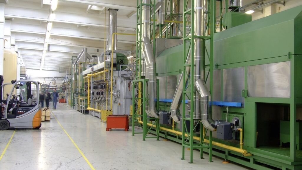
Semiconductor manufacturing facilities are experiencing significant changes. This shift is driven by the use of robotics in manufacturing, construction, and plant operations. The change is redefining workforce skills in demand and introducing new efficiencies, safety, and design factors. With accelerating fab automation, the structure of labor – both on the factory floor and behind the […]
3D IC Assembly Implications on Fab Layout
The transition to 3D Integrated Circuit assembly is an important step for the semiconductor evolution. Vertically stacking dies increases performance within less space, resulting in smaller energy-efficient devices. However, such advanced designs need fabrication facilities to extend beyond two-dimensional processes. Enabling 3D IC assembly requires hybrid packaging support, more stringent environmental control, and tool sets […]
How Degassing Equipment Improves Battery Cell Output
Battery manufacturing continues to be challenged by gas build-up. This build-up degrades electrochemical performance and stability. Trapped gases create voids, paths of resistance, and impede the contact between electrolytes and electrodes required for effective energy transfer. Specialized degassing equipment solves these issues through vacuum systems, controlled environments, and proprietary extraction techniques that work with all […]
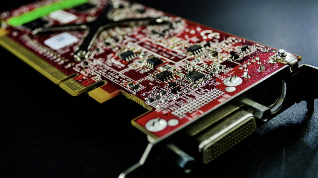
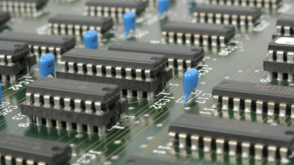
Semiconductor Manufacturing: Best Defect Reduction Strategies

Semiconductor manufacturing is done within tolerances measured in nanometers, where even small imperfections can make wafers worthless. The semiconductor industry is coming under increasing pressure to provide higher yields while coping with complex manufacturing processes on advanced node technologies. Leading-edge fabs are required to meet stringent quality demands with economical manufacturing. This makes defect reduction […]
What the CHIPS Act Means for U.S. Semiconductor Factories
Semiconductors are the core of modern technology. It powers everything from mobile phones to advanced defense systems. The US government passed the CHIPS and Science Act, recognizing the strategic value of chip fabrication as a part of a larger strategy to support domestic production. The act is a move to cut back on foreign dependence […]
Cyber-Physical Security Integration in Modern Fab Design
Semiconductor fabrication plants are heavily integrated production environments. This is where manufacturing precision confronts digital sophistication. The interoperability of operational technology and IT networks creates complex security threats. These require creative mitigation strategies. Furthermore, conventional security architectures isolating cybersecurity and physical threats reveal primary vulnerabilities in current manufacturing environments. Contemporary fab design requires converged security […]
ESD Control in Semiconductor Cleanroom Environments

Electrostatic discharge is among the most significant threats to semiconductor manufacturing. It costs billions of dollars’ worth of damage annually to the industry. New microprocessors and memory chips are constructed at nanoscale lengths where even minimal amounts of static electricity will irrevocably change delicate circuit patterns and junction structures. Semiconductor cleanroom environments, while in need […]
Digital Documentation Systems for Semiconductor Facilities
Paper-based documentation systems are challenged to cope with the continually increasing technical data in contemporary semiconductor plants. The capturing, storing, and recovering process of critical data in business organizations has been significantly transformed due to digitalization. Modern/digital documentation systems currently integrate AI, foresight analytics, and other frontier technologies into one comprehensive information ecosystem. Unlike traditional […]
EUV Lithography in Semiconductor Fabs
Extreme Ultraviolet (EUV) lithography is the cutting-edge semiconductor manufacturing tech. It makes way for the production of chips with elements under 7 nanometers. The process employs 13.5-nanometer light wavelengths to etch complex patterns of circuits into silicon wafers with unmatched accuracy. In addition, EUV lithography is becoming mainstream for leading foundries producing high-end processors, memory […]
Event Partners: 3rd Semiconductor Fab Design & Construction Summit – East Coast Edition
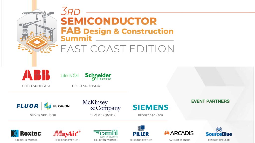
The 3rd Semiconductor Fab Design & Construction Summit – East Coast Edition is the essential forum for tackling the most pressing issues in semiconductor plant development. From managing complex supply chains to achieving sustainable design, the summit finds solutions that guarantee project success and operational efficiency. Attendees can gain access to proven methods, emerging technologies, […]