")

Dallas was full of energy and ideas at the 4th Semiconductor Fab Design & Construction Summit. The semiconductor industry is moving fast to meet global demand, and this summit brought together the people actually building the future of chip fabs. From new approaches in fab design to sustainable construction methods, the conversations focused on what it takes to create the next generation of manufacturing facilities.
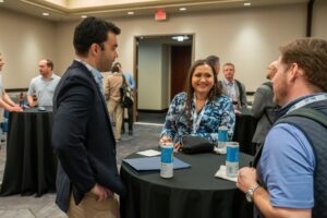
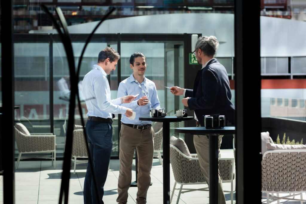
Outside the sessions, the event was alive with networking. Engineers, executives, and policymakers were all over the place, talking, swapping ideas, and figuring out solutions together. In this article, we’ll go over some of the most interesting sessions, see what the sponsors brought, and share a sense of what made the summit so special.
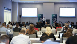
Sessions – 4th Semiconductor Fab Design & Construction Summit
At the sessions, experts shared their thoughts on design, efficiency, and sustainability in semiconductor fab design & Construction. They showed how new approaches in innovation and teamwork are shaping the fabs we’ll be building next. So, let’s take a look:
Workforce, Water Scarcity, & Wafer Fab Design
Speaker: Pablo Ruiz, Vice President, Austin Commercial
The presenter put emphasis on the complex relation that is there between workforce development, water availability, & wafer fab design efficiency. The discussion went through how modern fabs must evolve with new infrastructure models. Ones that optimize both sustainability & performance. Further, the speaker emphasized the critical demand for adaptable engineering strategies: these support environmental goals and maintain high-yield manufacturing. By drawing from decades of experience with construction/facility management, the session provided an in-depth perspective. This is on balancing operational goals with constraints of natural resources in fab environments.
The Modernization of 200mm Wafer Fabs
Speaker: Thomas Reamon, Module Manager, Texas Instruments
In this session, the speaker went through how lessons from 300mm wafer manufacturing can find application to optimize legacy 20mm fabs. In addition, the talk went on to speak about:
- Improving module-level productivity,
- Emissions reduction,
- & improvements in cycle times without infrastructure changes.
The speaker shared some hands-on ways to use automation, smart data tracking, and better process flows to get more life out of older fabs. The main point was that updating these facilities helps them stay competitive, even as the industry keeps moving fast. As a result, it ensures mature fabs can keep delivering high value within the global supply chain.
Maximizing Federal Incentives: R&D Credit, 48D ITC, CHIPS Grants, and DBA Compliance in Semiconductor Fab Construction
Speaker: Nick Panko, Vice President, CFO Services
This session at the 4th Semiconductor Fab Design & Construction Summit went through the financial side of semiconductor fab design & construction. It gives focus to how companies can maximize incentives given by the government. In addition to that, the speaker shared practical advice on:
- Navigating R&D credits
- Applying for CHIPS Act grants
- Understanding tax rules that can affect whether a project moves forward
The focus was on planning long-term finances in a way that keeps things on track. The session included real examples showing how handling these programs the right way can speed up construction, open up money for reinvestment, & make U.S. semiconductor projects more competitive.
FIRESIDE CHAT: AI-Driven Digital Twins – Speeding up Fab Design & Building Capabilities in Workforce
Speaker: Dr. Ehsan Azimi, Assistant Professor, University of Arizona
The discussion focused on digital twins and how they’re changing fab design and team training. With AI simulations, it’s possible to spot problems early and make smarter design choices before any construction begins. Using digital twins doesn’t just save time or money. They also help the workforce get better with data & feel confident using it in their work. So, this integration of human-AI collaboration is becoming a cornerstone in making smarter fabs that adapt to changing technologies and production issues.
Onsite Reclamation Technology to Reduce Waste Treatment Footprint, Water Usage, and Total Costs while Reducing Long-Term Regulatory Burden
Speaker: Austin Collins, Sales Director, ElectraMet
The session at the 4th Semiconductor Fab Design & Construction Summit was focused on how fabs can tackle waste/water challenges with onsite reclamation. Furthermore, the speaker explored how peroxide abatement makes way for the reuse of sulfuric acid and minimizes the treatment footprint of ammonia-peroxide mixtures. Moreover, there was an emphasis on recovering valuable materials such as copper, silver, gold, & palladium from concentrated & CMP waste. By combining these solutions, fabs can significantly cut down water discharge. They can also lower carbon emissions & ease the long-term regulatory pressure while minimizing operational costs.
Taking the Semiconductor Industry Toward Net Zero – Innovation, Efficiency, & Collaboration
Brainstorming Session
This brainstorming session focused on real/workable steps to help fabs cut emissions without making a dent in performance. Attendees were talking about putting renewables into power systems, and the idea is to keep energy costs from jumping around while also cutting down on carbon. They examined new process designs that reduce heat loss and improve the powerhouse during wafer fabrication. The conversation also scratched on supplier collaboration to make upstream materials more sustainable. So, rather than broad goals, the session drilled into measurable ways that link energy efficiency with cost savings/long-term competitiveness.
Upgrading Resilience in Semiconductor Supply Chains amid Global Shifts
Speaker: Deepshikha Shekhawat, Business Intelligence Program Manager – AMD
This session at the 4th Semiconductor Fab Design & Construction Summit discussed how supply chain stability has become the prime element in sustaining chip production amidst shifting global dynamics. In this regard, the speaker also elaborated on regional diversification and dual sourcing to minimize dependency on one supplier. Much emphasis was placed on restructuring the logistics framework to respond effectively to geopolitical disruptions and material shortages. Additionally, real-time digital tracking systems were also put in the spotlight to see supplier performance and inventory flow. The session further mentioned closer partnerships of manufacturers and raw material providers to secure crucial inputs over longer horizons.
Making Tomorrow’s Fab Floorplans – Scalable, Agile, Smart
Brainstorming Session
This brainstorming session at the 4th Semiconductor Fab Design & Construction Summit was a deep dive into how the physical/digital layers of a fab can work in tandem to make smarter production environments. Professionals examined how interlinked utility corridors, adaptive cleanroom zoning, & reconfigurable tool clusters could shorten ramp-up times for new nodes. Furthermore, they discussed how sensor intelligence can be embedded directly into the floorplate. This is to track vibration, contamination, and airflow in real time. At the same time, they talked about making the most of space and planning ahead so there’s less waste and the process stays smooth.
PANEL DISCUSSION: Modular Construction as the New Norm
Speakers: Julian Helmi, Senior Construction Project Manager / CTO, Microsoft / Prime Construction; Drew Overmiller, Vice President & Director of Engineering & Planning, JE Dunn Construction Company
The panel dug into how modular construction is transforming fab building from the ground up. The speakers were articulate on how factory-built modules for cleanrooms, HVAC, and utilities skids are helping projects move faster with more precision. They pointed out that putting parts together off-site keeps the site less crowded & improves quality while speeding up setup. It also means you need fewer people on-site and can save money – all without compromising on the technical side. Overall, the panel made a strong case when it comes to modular construction becoming the standard way for future fabs.
FIRESIDE CHAT: Designing Fabs for the Next Frontier – Making way for Radiation-Tolerant & Neuromorphic Electronics Manufacturing
Speaker: Dr. Bruce Gnade, Emeritus Professor, UT Dallas
The session delved into how FABs need to reimagine the production of chips that can thrive under radiation-rich conditions & implement brain-like computing. The speaker also explained how conventional process flows need to be reorganized to handle special materials. Wide-bandgap semiconductors, new types of interconnects, etc., were taken as examples. Moreover, the session discussed integrating shielding architectures into tool layouts. This maintains particle stability during exposure. Advanced cleanroom zoning and adaptive metrology were presented as methods to preserve device integrity during complex patterning steps. The talk took a conclusion by linking architectural foresight with breakthroughs in neuromorphic performance & radiation resilience.
Flexible Electronics & Eco-Conscious Engineering for High-Performance Systems for Manufacturing
Speaker: Dr. Dhruv Seshadri, Assistant Professor, Lehigh University
This session took into account the role played by flexibility and sustainability in redefining the performance/form/sustainability in advanced manufacturing. It was also discussed how other factors, like thin-film transistors, printed conductors, and organic semiconductors, make devices reliable even when put under mechanical stress. The speaker emphasized how these materials open new opportunities for wearables, adaptive sensors, & lightweight system architectures. Beyond product design, the session put a focus on engineering methods that reduce energy use/chemical intensity during fabrication. It gave a vision where environmental responsibility directly makes technological capability stronger.
Digital Twins in Semiconductor Construction and Operations
Speaker: Julian Helmi, Senior Construction Project Manager / CTO, Microsoft / Prime Construction
The speaker at the 4th Semiconductor Fab Design & Construction Summit focused on how digital twin technology is coming into use to bring greater precision and control to semiconductor projects. Moreover, it explored how virtual modeling supports project visualization, detailed planning, & early clash detection. This reduces costly design conflicts. The session also covered how connected systems make way for asset tracking & predictive maintenance. This helps teams spot issues before they disrupt operations. Finally, the speaker highlighted how collaboration platforms made on digital twins allow real-time progress reviews. This keeps every stakeholder in line throughout construction & operations.
Global Geopolitics & the Semiconductor Ecosystem – Risks, Realignments, & Opportunities
Brainstorming Session
The brainstorming session centered on how changing global alliances and trade policies are changing the landscape of semiconductors. Professionals discussed how export controls, regional subsidies, & national security priorities are redrawing supply routes & investment flows. Additionally, there was a deep conversation around the risks of over-dependence on particular regions for advanced materials/tooling. Attendees explored how localized manufacturing methods & cross-border collaborations could balance resilience with competitiveness. The session ultimately framed geopolitics not only as a source of disruption but also as a driver when it comes to new strategic opportunities.
Sponsors at the 4th Semiconductor Fab Design & Construction Summit
There are always larger happenings behind the scenes in every major event, and this summit was no different. The sponsors didn’t simply underwrite the event; they influenced its substantive content. All of them had something special to offer, and collectively, attendees were given an inside look at how various aspects of Semiconductor Fab Design & Construction converge. This segment profiles the sponsors that enabled the summit’s discussions to be genuinely practical and future-oriented:
CFO Services: A TRG Company – Bronze Sponsor
CFO Services stands to be a specialist firm that is dedicated to securing business incentives for complex industrial projects. With more than 30 years of experience, it helps clients in identifying and capturing federal & state-level credits. It includes R&D tax benefits & CHIPS Act grants. Moreover, the company stands out for its mix of in-depth expertise and advanced analytics platforms. At the 4th Semiconductor Fab Design & Construction Summit, the organization added insane value by offering clarity on financial frameworks that have a direct influence on large-scale fab construction. Additionally, their insights empowered attendees to go beyond engineering toward sustainable capital management & reinvestment strategies.
ATS Inc. – Exhibiting Partner
ATS Inc. is a global pioneer when it comes to fiberglass-reinforced plastic duct systems. These ensure fire-safe & corrosion-resistant cleanroom environments. Furthermore, with more than five decades of experience, the organization has shaped safety & air control standards in semiconductor manufacturing. Its PFAS-free FXP™ FRP ducts are trusted for reliability & compliance with international standards. During the summit, ATS Inc. shared its valuable experience in maintaining cleanroom integrity and sustainability. Their presence aided professionals in understanding how viral airflow engineering is to achieve high yield and safe operations when it comes to modern fab construction.
Victaulic – Exhibiting Partner
Victaulic is a global leader in mechanical pipe joining & flow control systems. It redefines piping installation for semiconductor manufacturing. By getting rid of traditional welding, Victaulic makes construction safer, cleaner, & faster – an essential advantage for fab conditions. Moreover, with over 2,000 patents all around the world, its solutions improve efficiency, lifecycle maintenance, & modularity. At the 4th Semiconductor Fab Design & Construction Summit, the company’s contribution was in demonstrating how mechanical joining technologies optimize the timelines of projects. This is while aligning with sustainability/safety goals. This inspired attendees to adopt innovative approaches to fab infrastructure.
ElectraMet – Presenting Partner
ElectraMet is revolutionizing water treatment for semiconductor manufacturing with electrochemical innovation. Their systems remove dissolved metals & oxidants without chemicals/membranes. This changes wastewater into a reusable resource. By combining sustainability with cost efficiency, the organization leads the movement toward circular water use in fabs. When it comes to the 4th Semiconductor Fab Design & Construction Summit, ElectraMet showcased how advanced reclamation technologies can turn environmental challenges into operational strengths. Additionally, their participation highlighted the crucial link that is present between eco-innovation & long-term resilience of semiconductor facilities.
To Sum Up
The 4th Semiconductor Fab Design & Construction Summit reflected how deeply the industry is evolving – Be it technically, environmentally, & strategically. Every session & partnership was showing the shared goal of designing/constructing fabs that are efficient, sustainable, & future-proof. When we see events like this, they are not just about learning; they are about connecting ideas & professionals who will define the next era of chip production.
Attendance at such forward-focused industry summits is the smartest move you can make today to stay ahead of the curve and lead innovation in your industry. Sounds like something you are aligned with? Click here to learn more!