Semiconductor Facilities, Operations & Expansion. The definitive gathering of manufacturers, fab owners, EPC contractors, engineers and technology providers delivering America's advanced fabs, faster.
Engineering the Facilities Behind America's Chip Supply
The 8th Semiconductor Design, Construction & Engineering Summit brings together semiconductor manufacturers, fab owners, EPC contractors, engineers, technology providers and industry leaders to address the challenges and opportunities shaping the next generation of U.S. chip manufacturing.
As domestic manufacturing capacity continues to expand, the industry faces increasing pressure to deliver advanced facilities faster, strengthen supply chains, secure skilled talent, and build the resilient infrastructure required to support increasingly sophisticated production environments. From advanced packaging and High-NA EUV readiness to mega-fab project execution, utility infrastructure and cleanroom engineering, organisations are rethinking how semiconductor facilities are designed, constructed and commissioned.
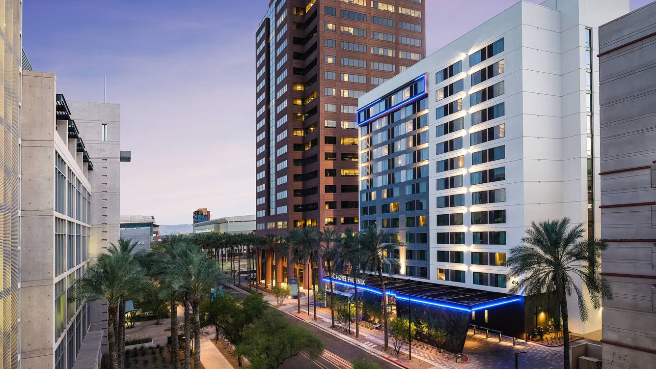
Taking place in Phoenix, Arizona — one of the world's most dynamic semiconductor hubs — the summit provides a platform for sharing practical insights, lessons learned and proven strategies for achieving engineering excellence and successful project delivery. Through expert-led discussions and peer-to-peer exchange, attendees will gain valuable perspectives on the priorities defining the future of semiconductor manufacturing.
Program Highlights
- Mega-Fab Construction & Delivery
- AI & HBM Manufacturing
- Advanced Packaging
- High-NA EUV Readiness
- Fab Expansion & Construction
- Supply Chain Resilience
- Manufacturing Equipment Integration
- Facility Operations & Ramp-Up
- Digital Twins & Yield Improvement
- Capital Project Optimisation
- Cleanrooms & Environmental Control
- Critical Utilities & Infrastructure
- Power & Energy Resilience
- Water Management & Sustainability
- Brownfield Expansion & Retrofits
- Compliance & Risk Management
- Workforce Development
- U.S. Semiconductor Growth & Competitiveness
Topics to Be Discussed
Comprehensive coverage of the most critical challenges and innovations shaping semiconductor facility design, construction and operations.
- How can semiconductor mega-fab projects be delivered faster while maintaining quality, safety and operational performance?
- What project delivery models best reduce cost overruns and schedule delays?
- How can organizations improve capital project governance across large-scale investments?
- How are AI-driven semiconductor investments reshaping fab design and construction?
- What infrastructure is required to support high-bandwidth memory manufacturing?
- What manufacturing challenges will define the next generation of AI chip production?
- What facility requirements are needed to scale advanced packaging?
- How should fabs prepare for High-NA EUV implementation?
- How can facilities remain flexible for future technology nodes?
- How can semiconductor facilities achieve faster production ramp-up?
- What best practices ensure successful commissioning and operational readiness?
- What strategies reduce startup risks for new fabs?
- How are digital twins transforming semiconductor facilities?
- How can AI and smart manufacturing improve production yield?
- What role does predictive maintenance play in fab performance?
- How can cleanroom environments meet increasingly demanding requirements?
- What HVAC innovations improve contamination control?
- How can humidity control maximize yield and process stability?
- How can manufacturers secure reliable power for future expansion?
- What strategies improve energy resilience and reduce operational risk?
- How can facilities reduce water consumption while maintaining quality?
- How can existing fabs be expanded without disrupting production?
- What are the biggest challenges in modernizing aging facilities?
- What strategies minimize operational risks during expansion projects?
- How can semiconductor manufacturers strengthen supply chain resilience?
- What strategies reduce project risk across major capital investments?
- How can organizations attract and retain skilled talent?
Built for the Teams Delivering U.S. Fabs
From C-suite executives to directors, heads and managers — the summit brings together every function responsible for designing, building and operating America's semiconductor facilities.
C-Level Officer, Vice-Presidents, Senior Vice-Presidents, Directors, Heads, Leaders, Managers and Etc.
Industries Represented
- Semiconductor Manufacturers & Foundries
- Integrated Device Manufacturers (IDMs)
- Advanced Packaging & Test Providers
- Fabless Semiconductor Companies
- Construction & EPC Contractors
- Architecture, Engineering & Design Firms
- Semiconductor Equipment Manufacturers
- Material & Chemical Suppliers
- Utilities & Energy Providers
- Water Infrastructure Companies
- Technology & Automation Providers
- EDA & Semiconductor Design Software
- Federal, State & Local Government
- Private Equity & Infrastructure Investors
- Supply Chain & Logistics Providers
Ample Opportunities, By Future Bridge
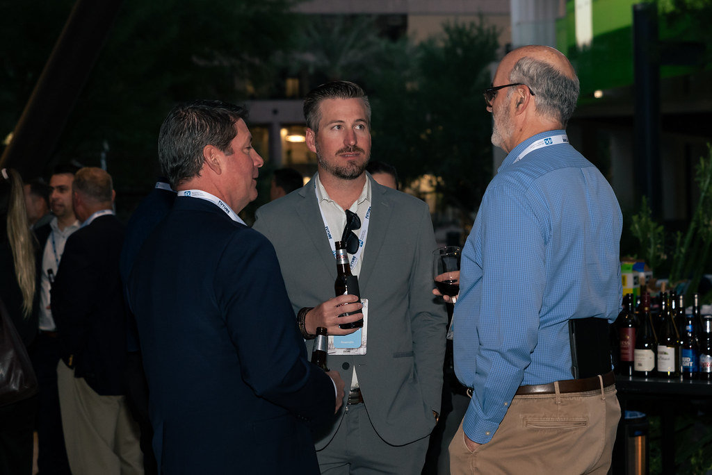
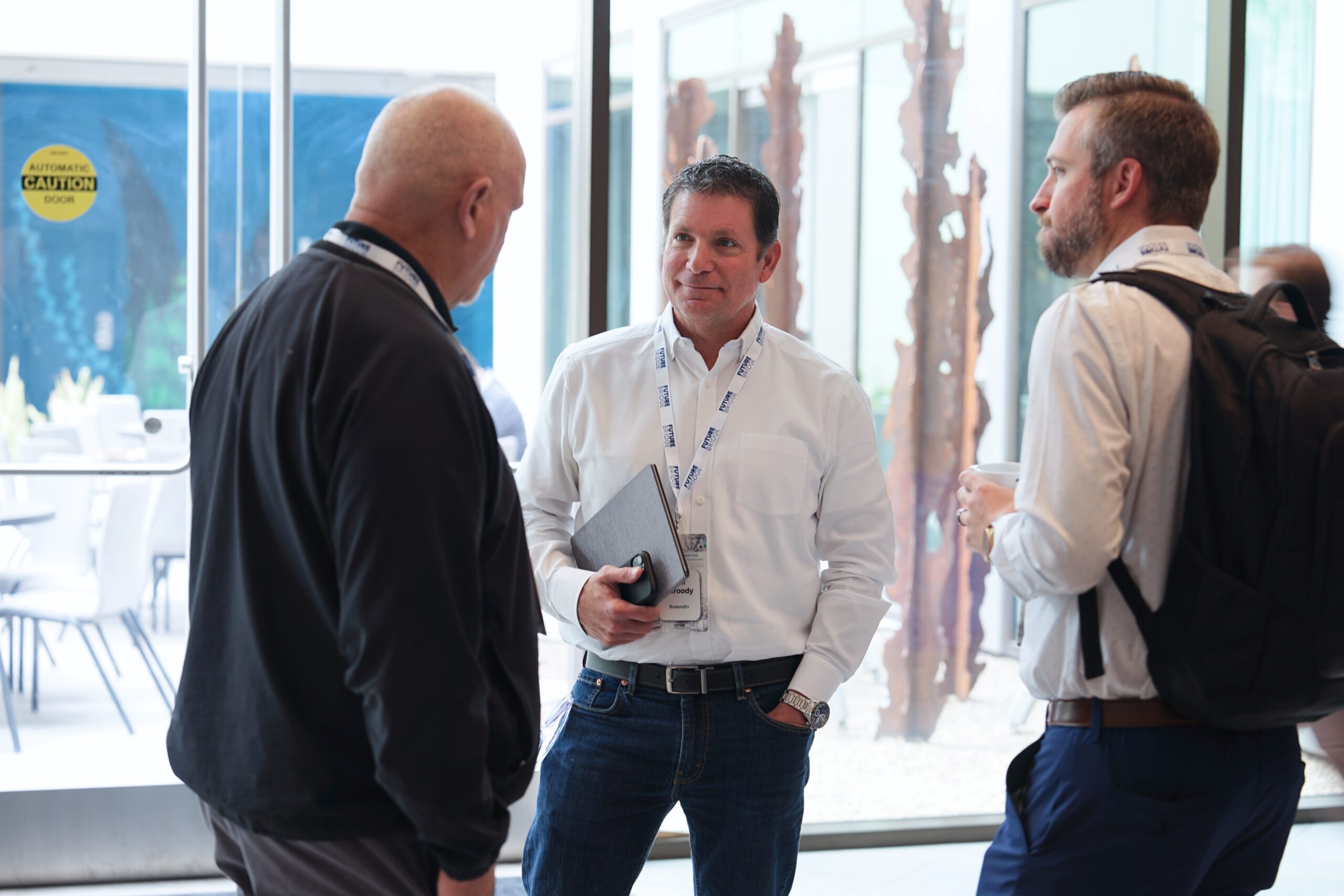
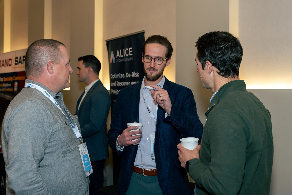
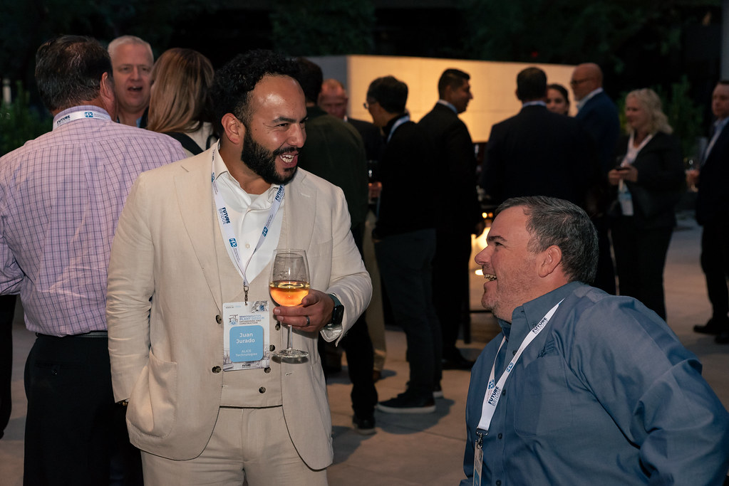
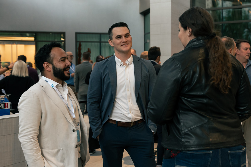
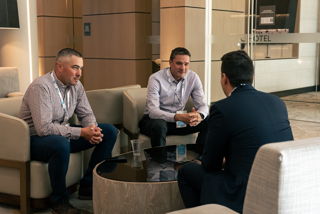
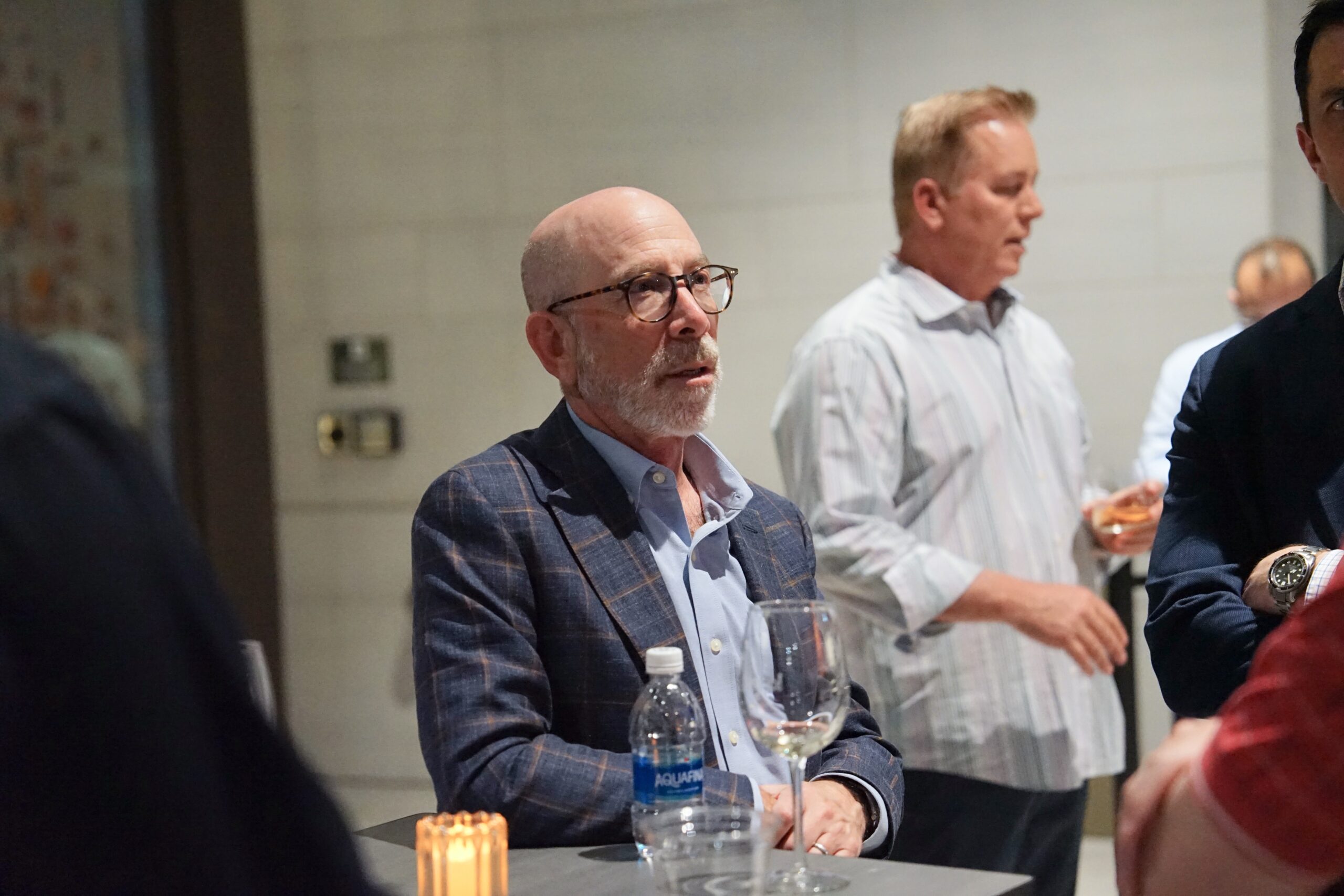
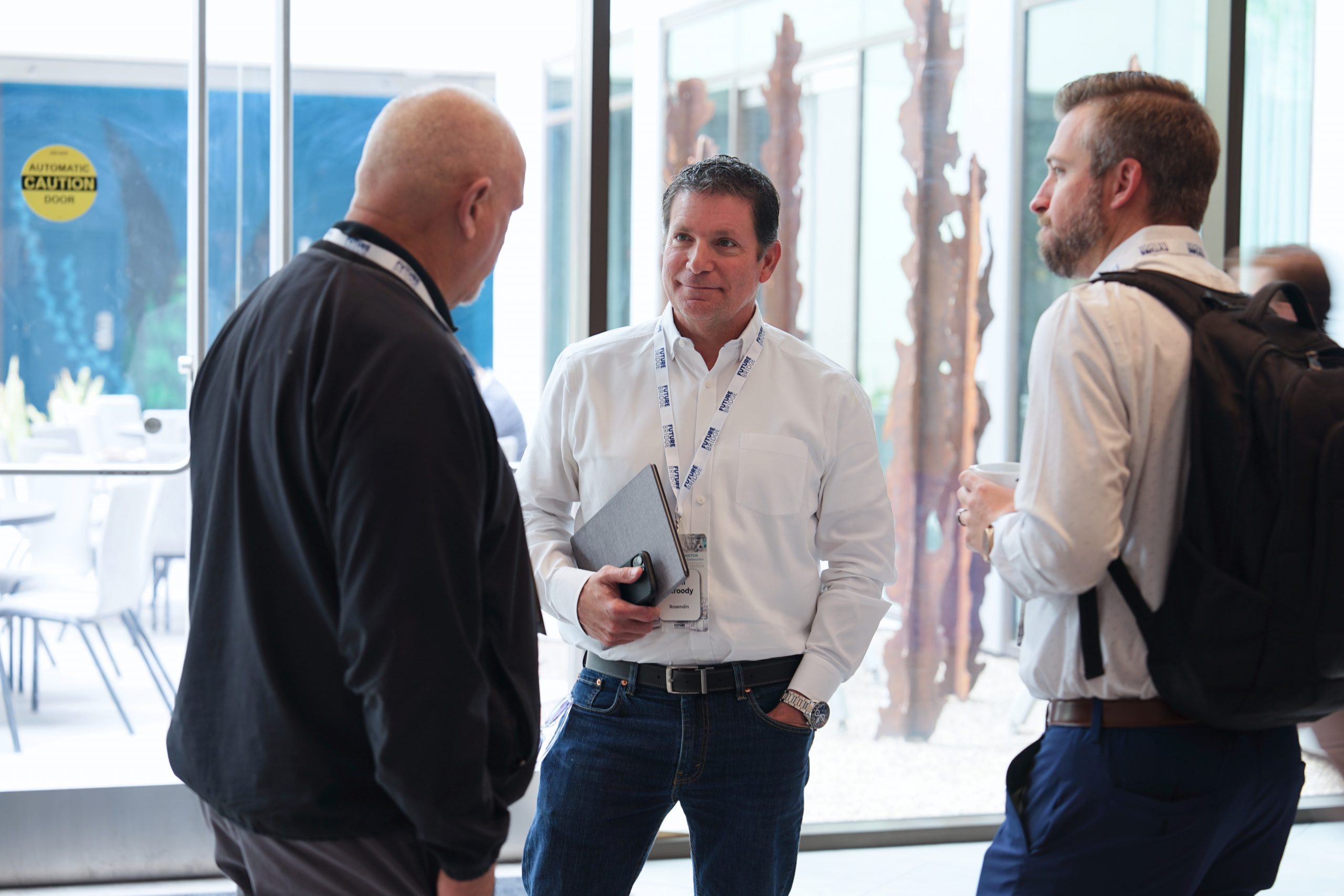
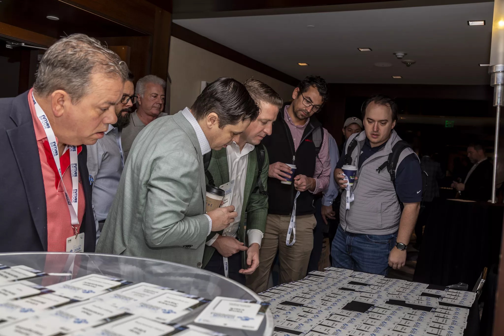
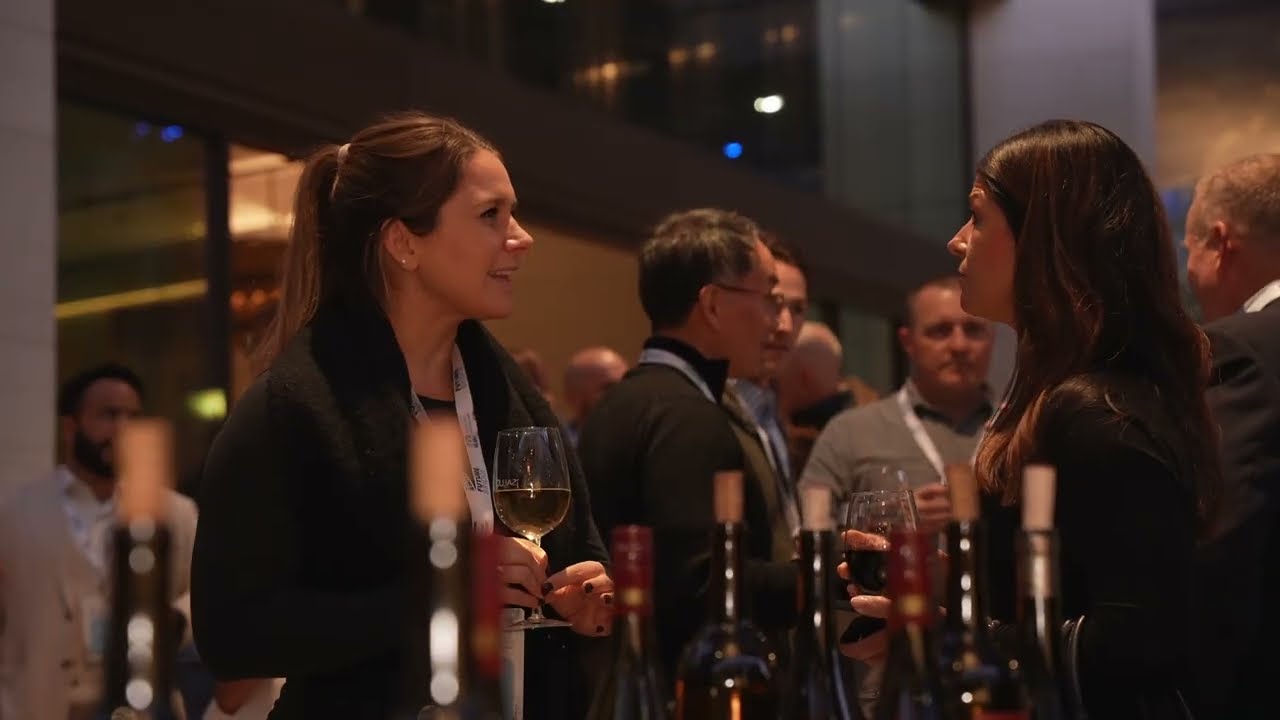
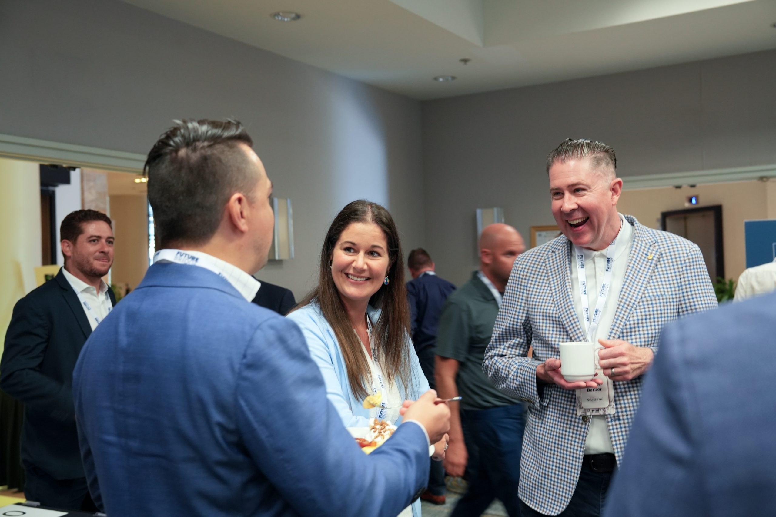
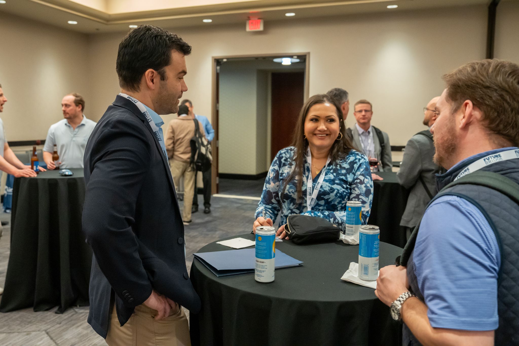
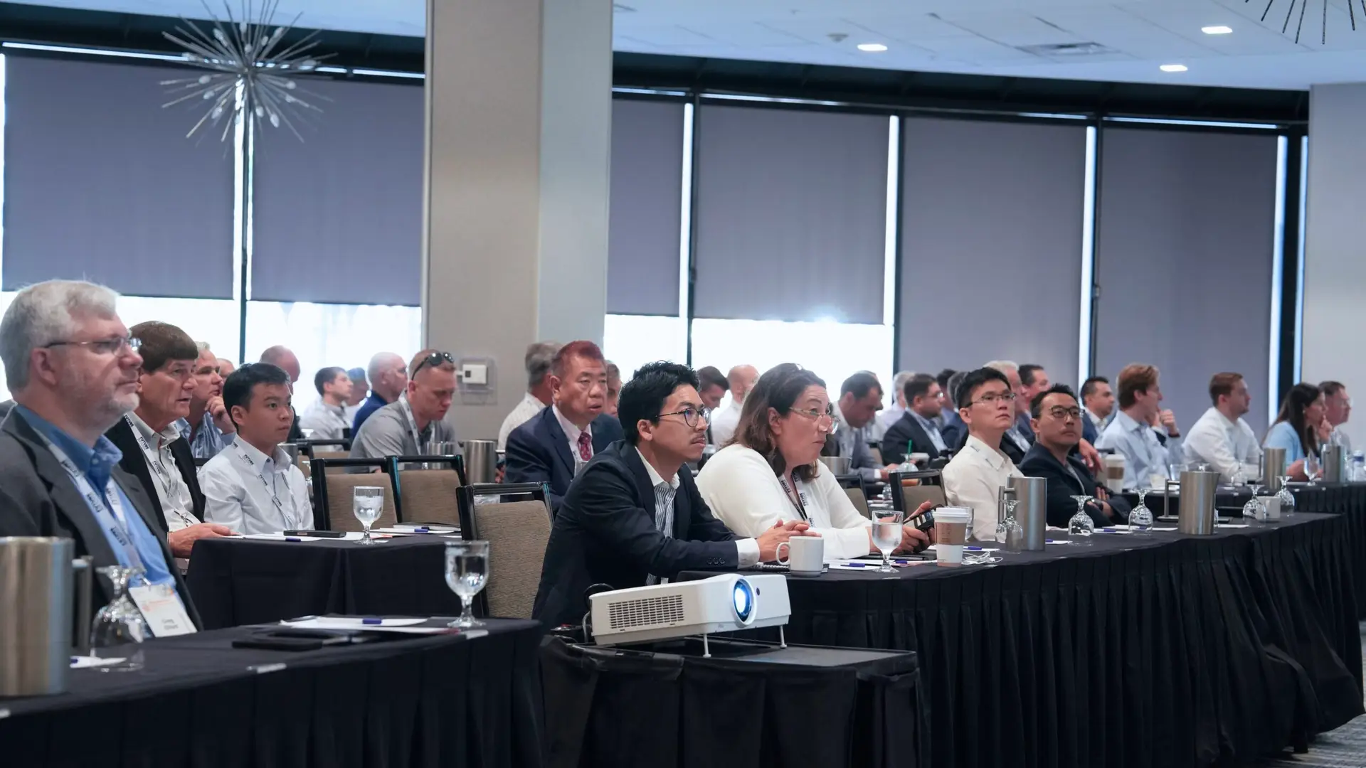
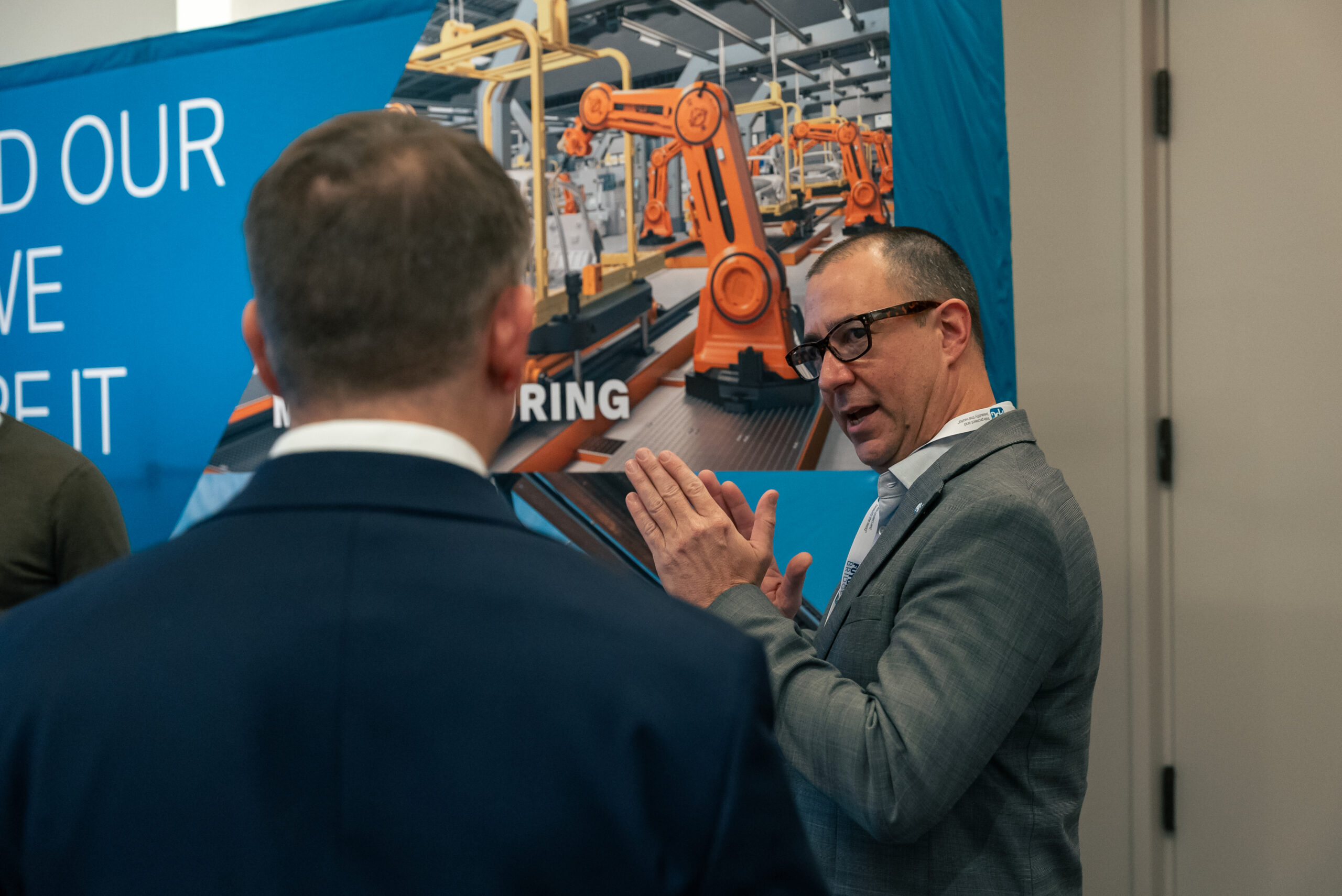
Future Bridge is proud to offer ample networking opportunities during our event. The agenda includes networking breaks featuring face-to-face meetings during coffee and ice-breaking sessions, designed to foster meaningful connections and facilitate interactions among attendees.
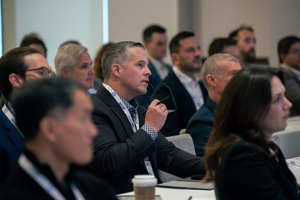
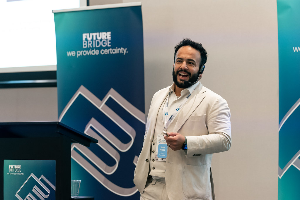
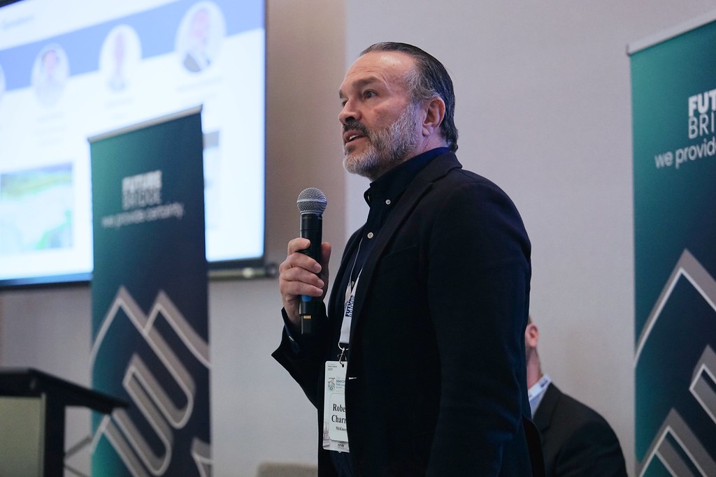
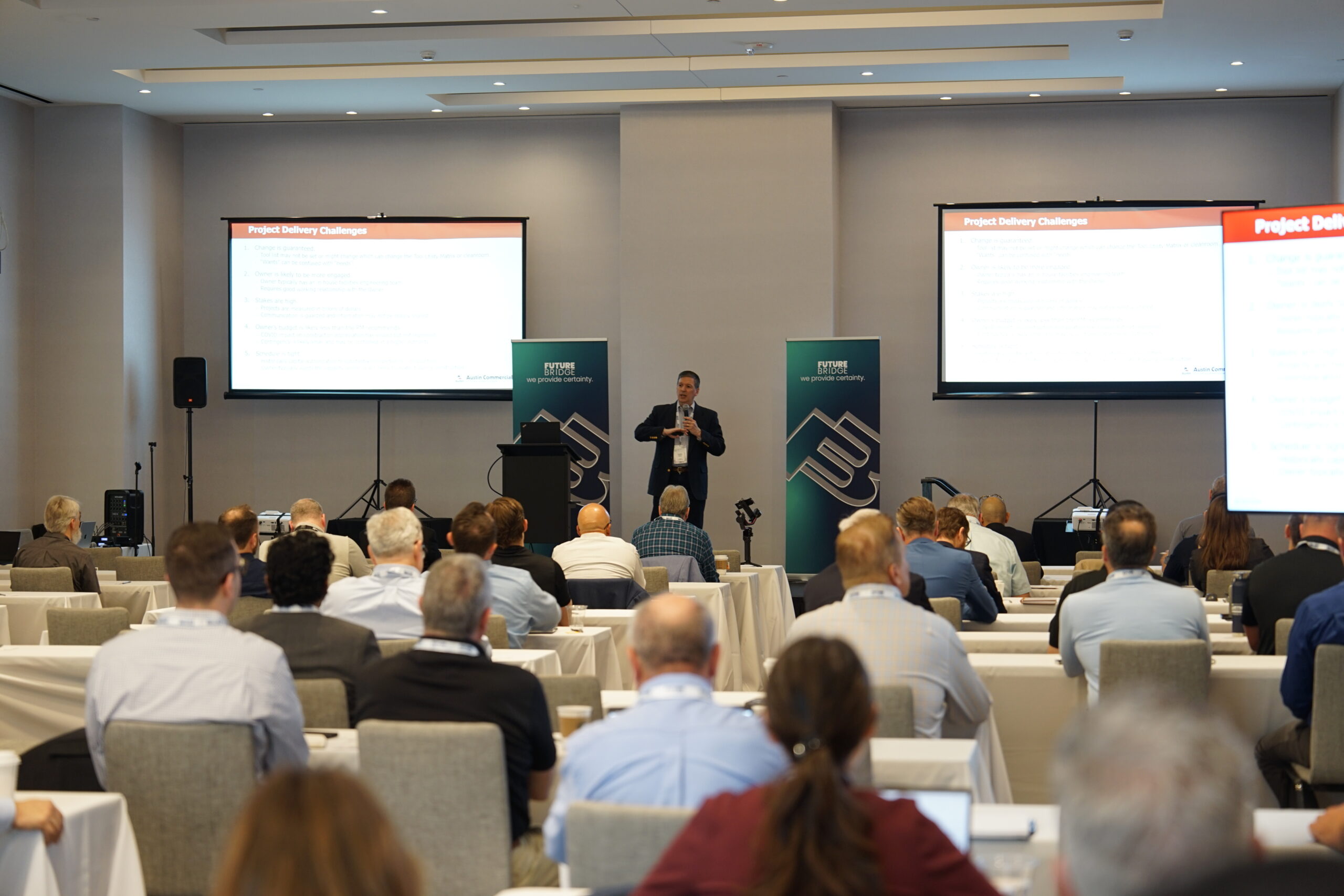
From Previous Summits
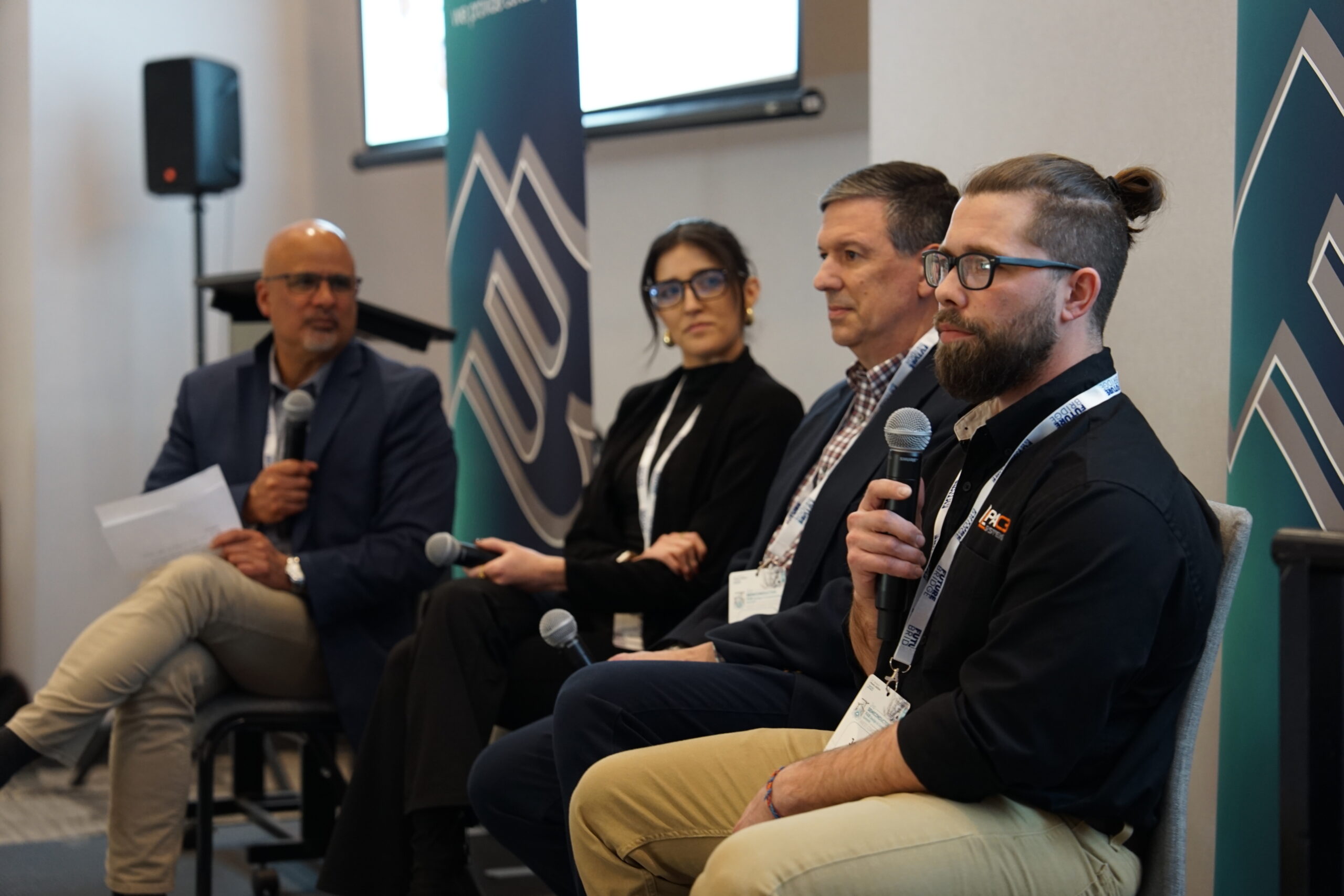
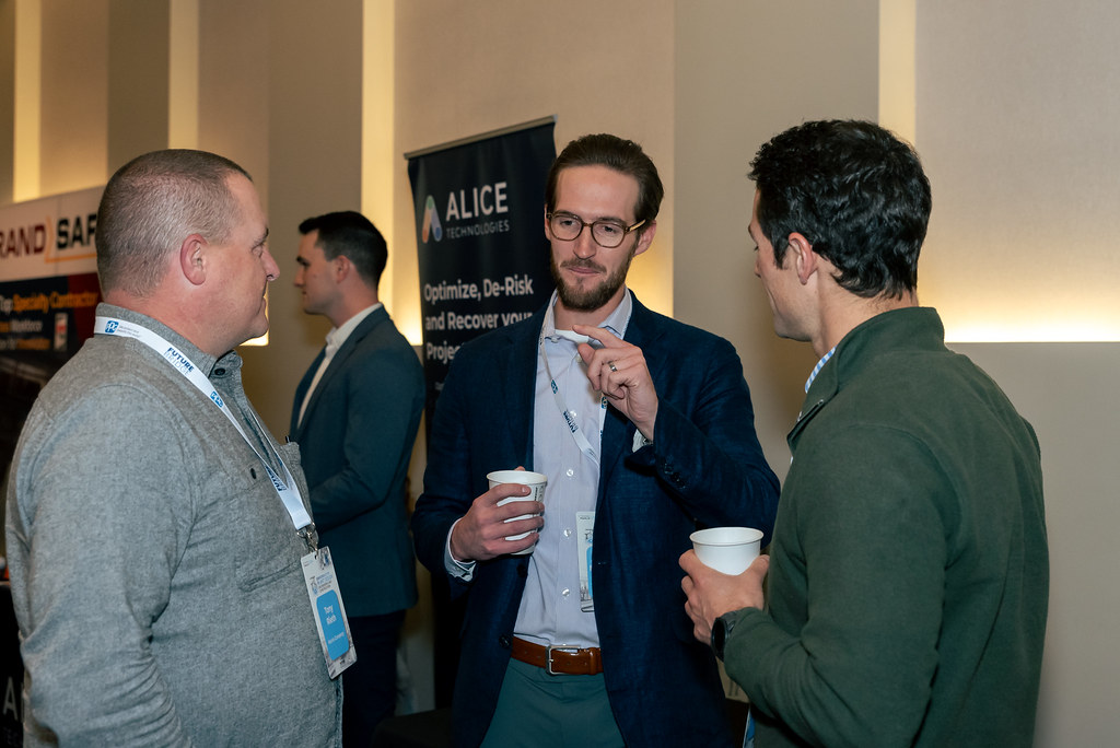
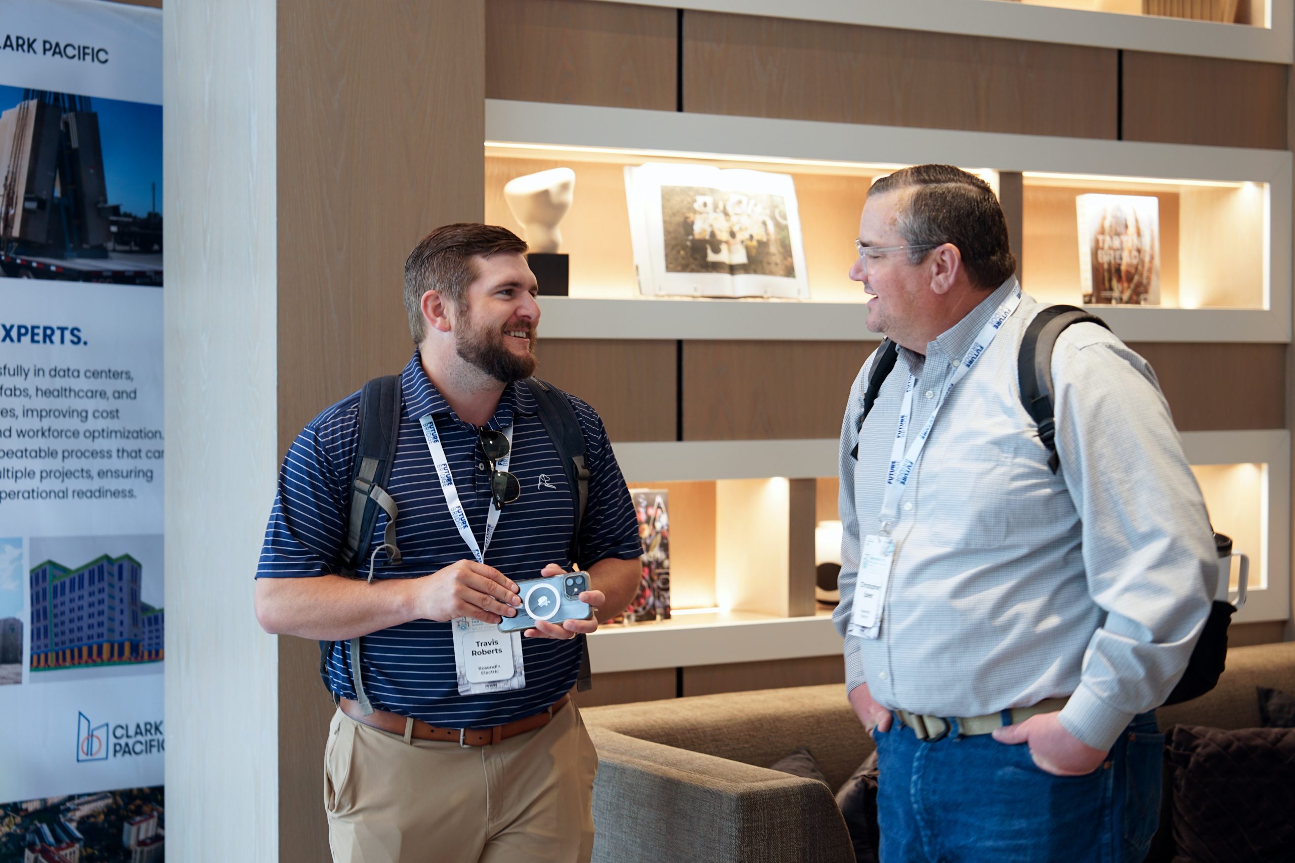
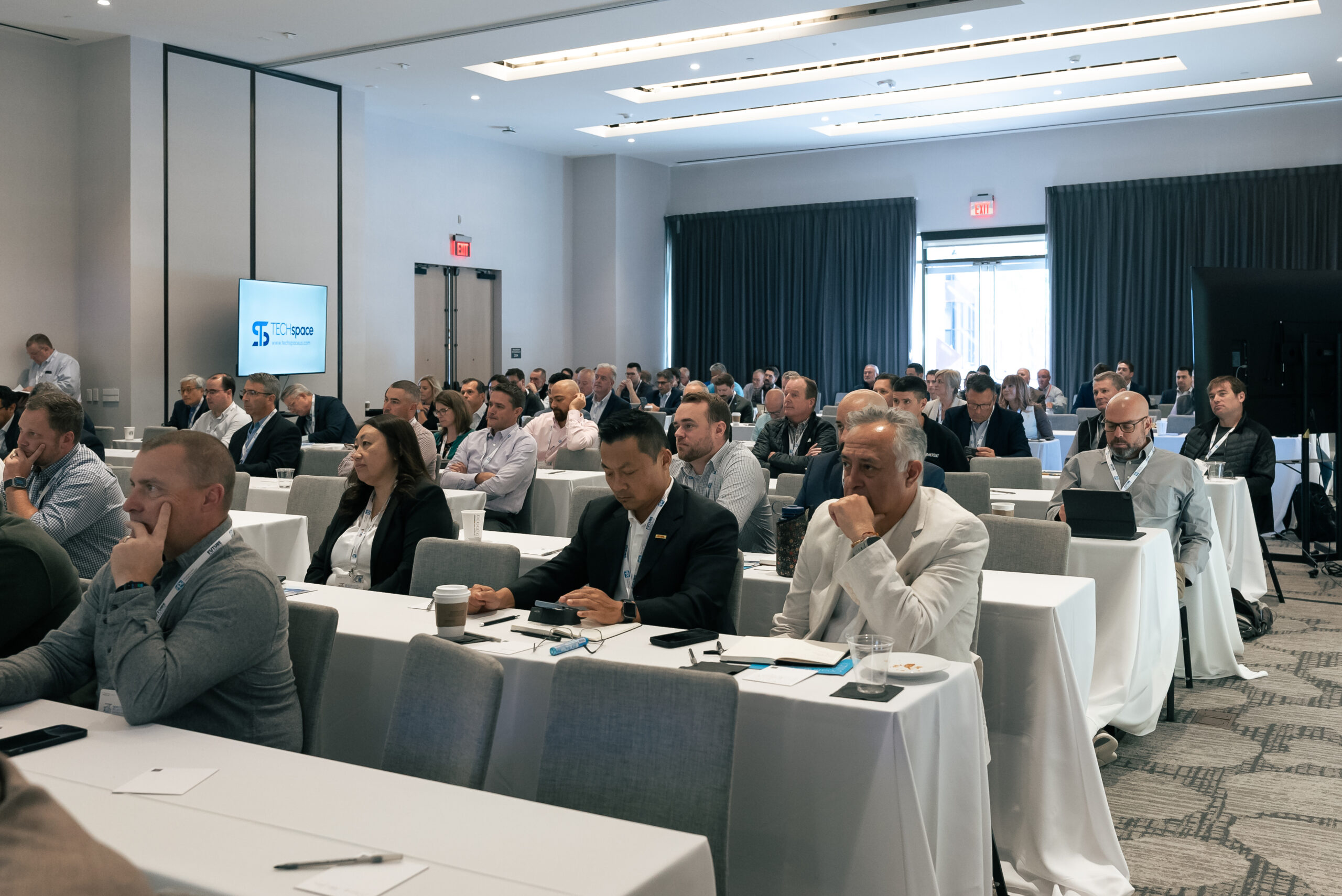
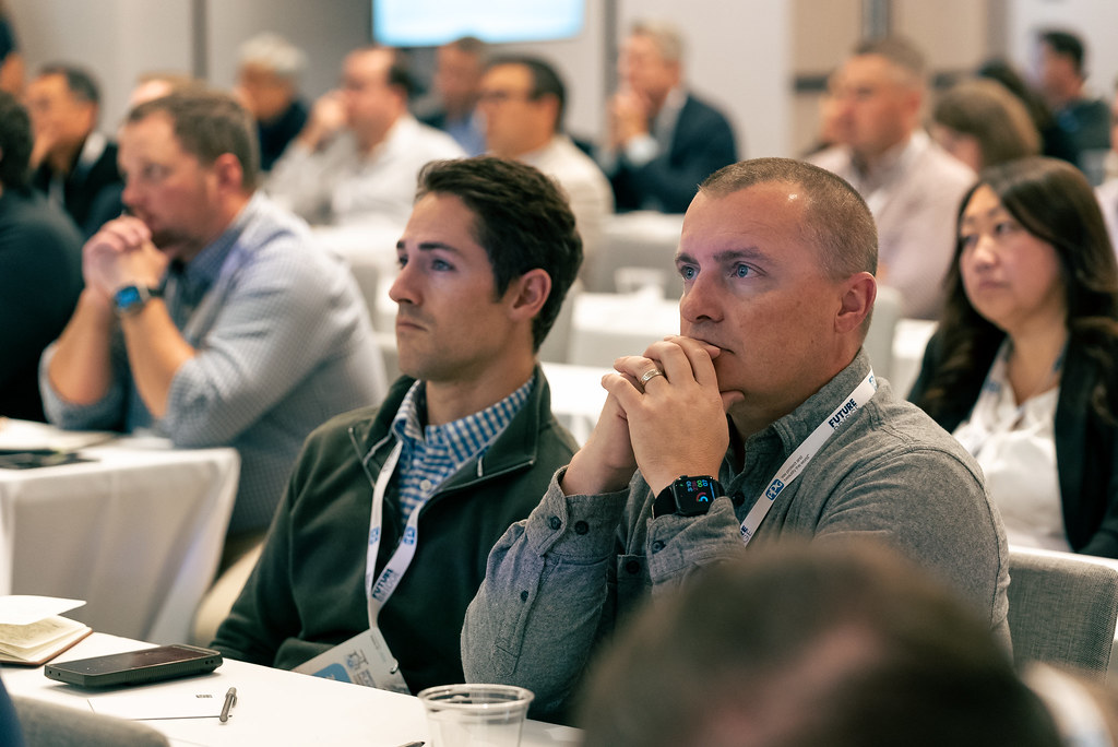
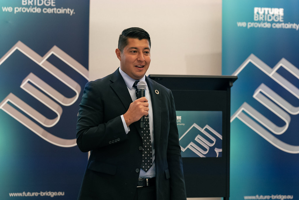
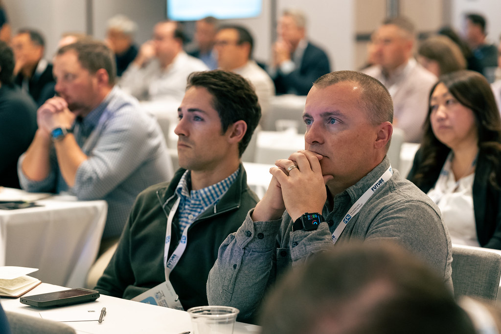
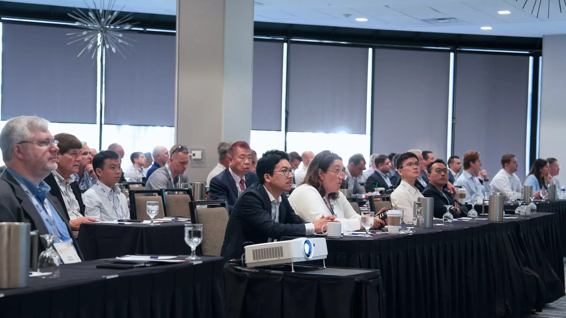
Participants will have the opportunity to engage in focused discussions, exchange ideas, and establish new relationships during both structured sessions and informal breaks throughout the two-day program.
Secure Your PlaceTrusted by Industry Partners
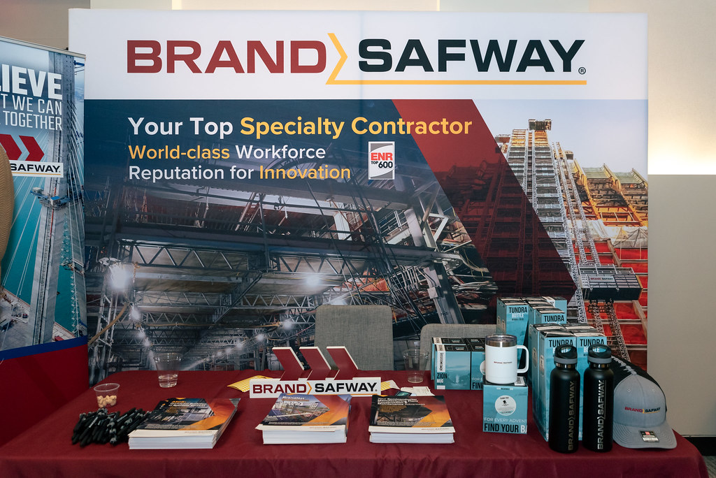
Exhibiting Partner
Don't Miss This Opportunity
Gain cutting-edge knowledge and connect with industry innovators shaping the future of semiconductor manufacturing.
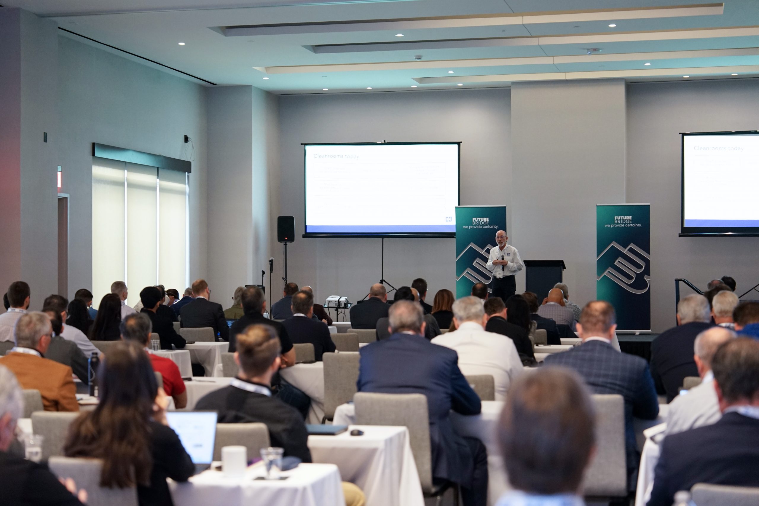
Highlights from the Semiconductor Plant Design, Engineering & Construction Summit
Get the Full Agenda
Access the complete programme — topics, format details, sponsorship packages and registration information for the 8th U.S. Semiconductor Summit.

Secure Your Place in Phoenix
Hotel accommodation and travel costs are not included in the registration fee.
- 2-Day Conference Pass
- Documentation Package
- Panel Discussions
- Refreshment Breaks & Lunches
- Drinks Reception
- Face-to-Face Networking
- Digital Certificate of Attendance
- 2-Day Conference Pass
- Documentation Package
- Panel Discussions
- Refreshment Breaks & Lunches
- Drinks Reception
- Face-to-Face Networking
- Digital Certificate of Attendance
- 2-Day Conference Pass
- Documentation Package
- Panel Discussions
- Refreshment Breaks & Lunches
- Drinks Reception
- Face-to-Face Networking
- Digital Certificate of Attendance
The 8th U.S. Semiconductor Design, Construction & Engineering Summit provides an excellent platform to elevate your company's profile within the semiconductor manufacturing and facility infrastructure sector, showcase your innovative solutions, and enable high-value networking with key decision-makers.
a Platform to:
Showcase. Connect. Lead.
- Exhibition stand space (1–2 roll-up banners in the networking area)
- 2 Delegate passes — full conference access
- Logo & company text in all conference materials, agenda, social media posts, and marketing emails
- Conference documentation package — all speaker presentations
- Speaker slot on the main conference program
- 1 Speaker attendee pass
- Logo & company text in all conference materials
- Conference documentation package — all speaker presentations
[email protected]
What Past Attendees Say
Hear from attendees of previous Future Bridge semiconductor summits as they share their experiences, insights and key takeaways — from networking opportunities to thought-provoking sessions led by industry experts.
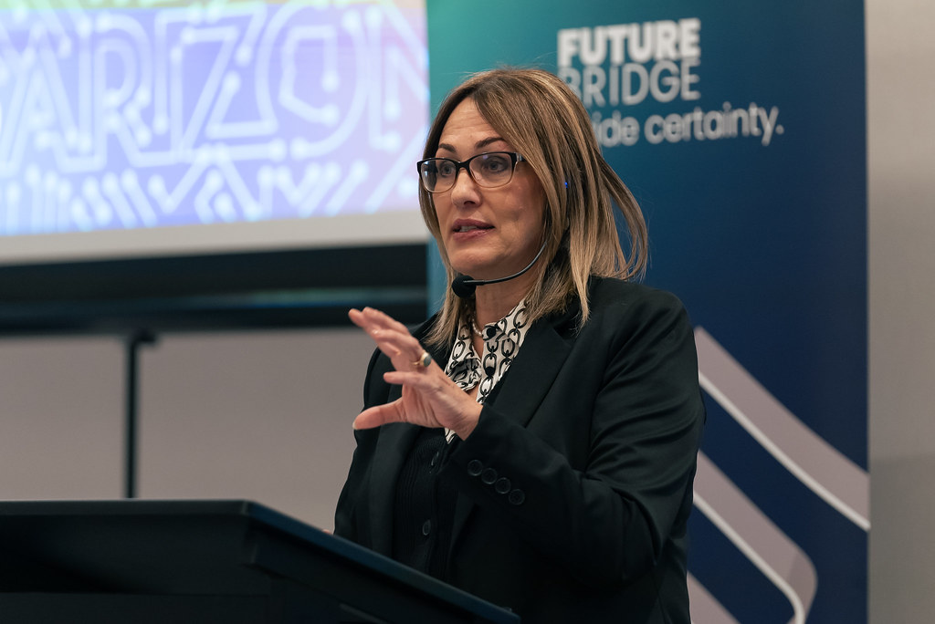
From Previous Semiconductor Design, Construction & Engineering Summits
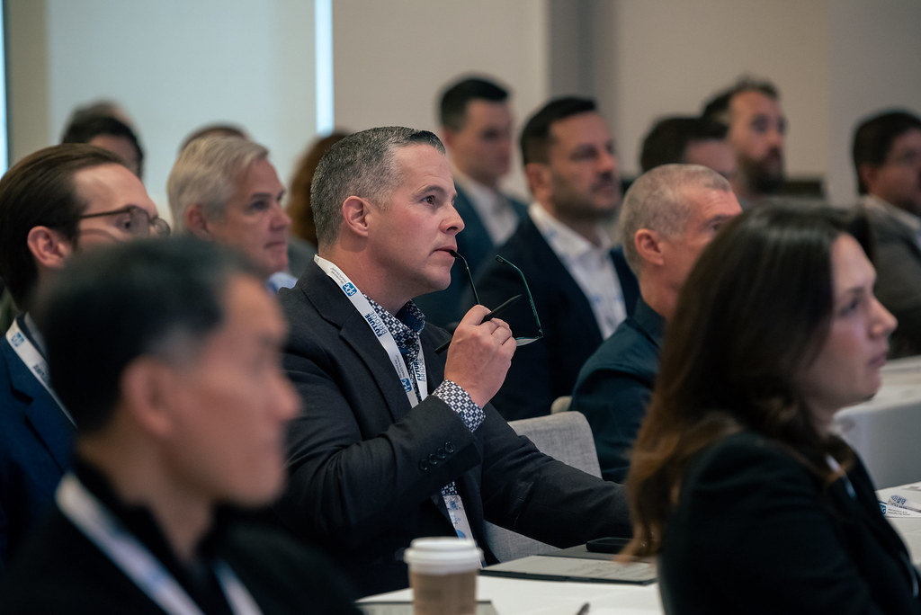
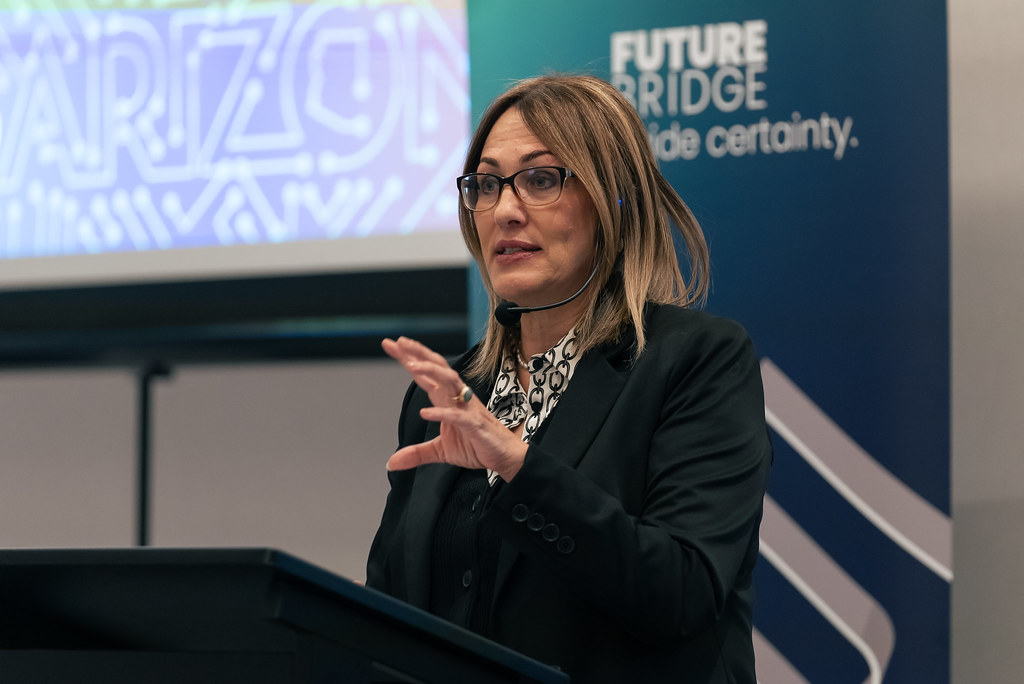
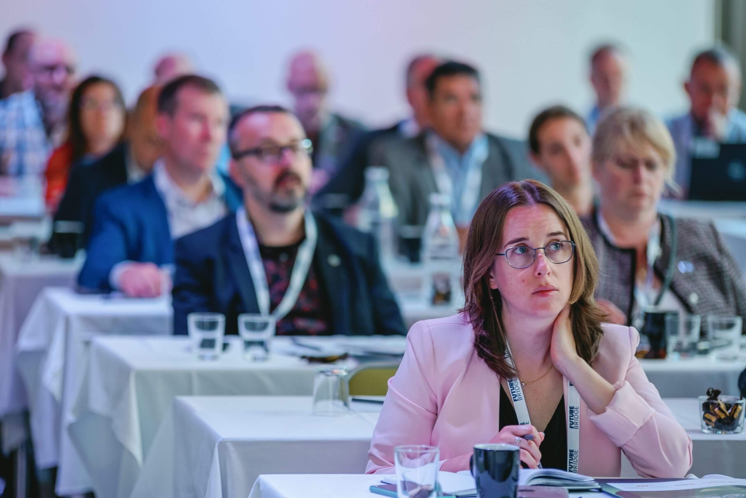
Highlights from our previous summits — connecting the semiconductor fab design and construction community across multiple editions.
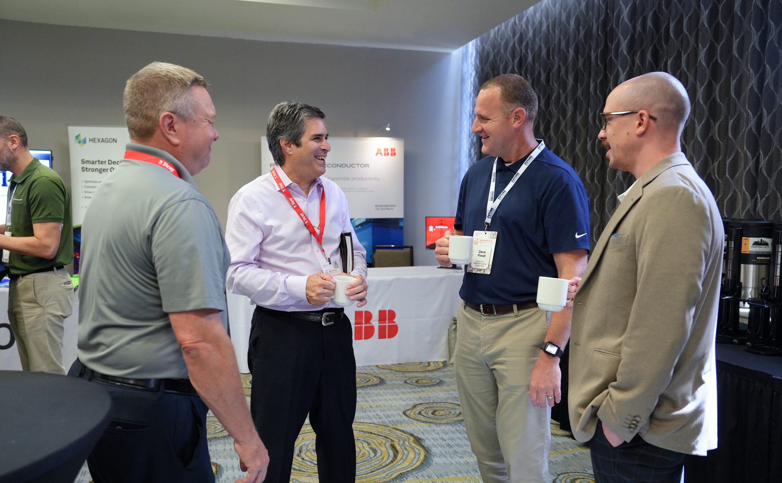
Where the Industry Connects. Collaborates. Builds.
Up to 6 hours of dedicated networking — coffee breaks, a drinks reception, and peer-to-peer sessions bringing together semiconductor fab leaders.
Secure Your Place