
Building a semiconductor facility involves thousands of decisions before production can begin. Power has to be available when the site needs it. Exhaust systems must handle heat and corrosive materials. Equipment and piping also need clear identification once the facility is running.
These requirements become more demanding as fabs grow larger and manufacturing processes become more advanced. The 8th US Semiconductor Design, Construction & Engineering Summit will examine many of these practical challenges. The agenda covers mega-fab construction, advanced packaging, AI and HBM manufacturing, cleanrooms, critical utilities, power, water management and facility operations. It also looks at brownfield expansion and the work needed to bring new facilities into production. This article looks at three companies whose products and services support different parts of this wider infrastructure.
What is Different in the 8th US Semiconductor Design, Construction & Engineering Summit
The summit covers the full facility lifecycle rather than focusing only on construction. Its agenda moves from project delivery and facility design to commissioning, production ramp-up and ongoing operations.
Several sessions deal with issues that can affect a fab long after construction starts. These include cleanroom conditions, critical utilities, power resilience and water management. The programme also addresses equipment integration, digital twins and brownfield expansion. Advanced packaging and High-NA EUV readiness are included as well. This gives the discussions a practical focus on the systems that allow semiconductor facilities to operate as intended.
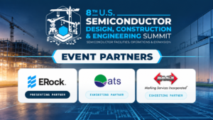
Event Partners: 8th US Semiconductor Design, Construction & Engineering Summit
The three companies work in different parts of facility infrastructure, from power generation to exhaust systems and asset identification.
ERock – Presenting Partner
ERock provides onsite power systems for manufacturers and other facilities that need dependable electricity. Its systems can supply power before a permanent grid connection is available. ERock calls this approach bridge power. Once a facility connects to the grid, the onsite system can continue supporting the site during periods of high demand or a grid failure.
The company uses natural gas generators in its onsite systems. It also provides engineering, procurement, and construction services. These services cover greenfield projects and upgrades to existing sites. ERock handles much of the work in-house, including design, engineering, production, testing, and deployment. Its manufacturing facility in Houston brings assembly, testing, and engineering together under one roof. For semiconductor projects, this type of power infrastructure can help address the electricity requirements of large manufacturing operations and the delays that can come with grid connections.
ATS Products, Inc. – Exhibiting Partner
ATS Products, Inc. has been making fiberglass duct systems since 1971. Its main focus is exhaust ductwork for industries where fire and corrosion are serious concerns. The company supplies round, rectangular, and oval FRP ducts, with its FXP range available in sizes from 2 to 160 inches. ATS also makes fittings such as elbows, tees, dampers, blastgates, and flanges.
Semiconductor manufacturing is one of the industries ATS serves. Its cleanroom exhaust systems are built to handle high temperatures and corrosive substances. The company also makes StaticSafe Duct for exhaust applications involving flammable or explosive gases. The system uses a conductive liner to dissipate static charge and has FM 4922 and FM 4910 approvals.
Marking Services, Inc. (MSI) – Exhibiting Partner
Marking Services, Inc. (MSI) deals with something easy to overlook during a large construction project: knowing exactly what each pipe, valve, and piece of equipment is. The company manufactures pipe markers, equipment and valve tags, safety signs and other asset labels. It also provides the engineering and installation work needed to put a labelling system in place.
Its engineering process starts with the project’s P&IDs. MSI uses them to prepare line lists containing details such as the contents of a pipe, its origin and destination, line number and flow direction. Engineers then walk the site to check those details against what has actually been installed. The company can keep the updated information in a facility asset database and record later changes. MSI says it has also used this approach on semiconductor facilities.
To Sum Up
The US semiconductor industry is building larger and more advanced manufacturing facilities. At the same time, project teams have to deal with power availability, tighter construction timelines, new manufacturing technologies, and the demands of high-volume production. These changes are making coordination between design, engineering, construction, and operations more important than ever.
The 8th US Semiconductor Design, Construction & Engineering Summit will take place on 4-5 November 2026 at the AC Hotel Phoenix Downtown in Phoenix, Arizona, USA. The event will bring industry professionals together to discuss the challenges shaping semiconductor facility development in the US.